- 您现在的位置:买卖IC网 > PDF目录98176 > TC7116IPL 1-CH DUAL-SLOPE ADC, PDIP40 PDF资料下载
参数资料
| 型号: | TC7116IPL |
| 元件分类: | ADC |
| 英文描述: | 1-CH DUAL-SLOPE ADC, PDIP40 |
| 封装: | PLASTIC, DIP-40 |
| 文件页数: | 31/32页 |
| 文件大小: | 515K |
| 代理商: | TC7116IPL |
第1页第2页第3页第4页第5页第6页第7页第8页第9页第10页第11页第12页第13页第14页第15页第16页第17页第18页第19页第20页第21页第22页第23页第24页第25页第26页第27页第28页第29页第30页当前第31页第32页
TC7106/A/TC7107/A
DS21455C-page 8
2006 Microchip Technology Inc.
3.0
DETAILED DESCRIPTION
(All Pin designations refer to 40-Pin PDIP.)
3.1
Dual Slope Conversion Principles
The TC7106A and TC7107A are dual slope, integrating
Analog-to-Digital Converters. An understanding of the
dual slope conversion technique will aid in following the
detailed operation theory.
The conventional dual slope converter measurement
cycle has two distinct phases:
Input Signal Integration
Reference Voltage Integration (De-integration)
The input signal being converted is integrated for a
fixed time period (TSI). Time is measured by counting
clock pulses. An opposite polarity constant reference
voltage is then integrated until the integrator output
voltage returns to zero. The reference integration time
is directly proportional to the input signal (TRI). See
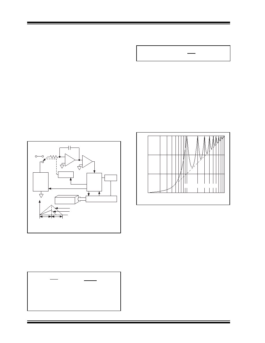
FIGURE 3-1:
Basic Dual Slope Converter
In a simple dual slope converter, a complete conver-
sion requires the integrator output to “ramp-up” and
“ramp-down.” A simple mathematical equation relates
the input signal, reference voltage and integration time.
EQUATION 3-1:
For a constant VIN:
EQUATION 3-2:
The dual slope converter accuracy is unrelated to the
integrating resistor and capacitor values as long as
they are stable during a measurement cycle. An inher-
ent benefit is noise immunity. Noise spikes are
integrated or averaged to zero during the integration
periods. Integrating ADCs are immune to the large
conversion errors that plague successive approxima-
tion converters in high noise environments. Interfering
signals with frequency components at multiples of the
averaging period will be attenuated. Integrating ADCs
commonly operate with the signal integration period set
to a multiple of the 50/60Hz power line period (see
FIGURE 3-2:
Normal Mode Rejection of
Dual Slope Converter
+
–
REF
Voltage
Analog
Input
Signal
+
–
DISPLAY
Switch
Driver
Control
Logic
Integrator
Output
Clock
Counter
Polarity Control
Phase
Control
VIN VREF
VIN 1/2 VREF
Variable
Reference
Integrate
Time
Fixed
Signal
Integrate
Time
Integrator
C
Comparator
+/–
1
RC
VRTRI
RC
TSI
0
VIN(t)dt =
∫
Where:
VR = Reference voltage
TSI = Signal integration time (fixed)
TRI = Reference voltage integration time (variable).
VIN = VR
TRI
TSI
30
20
10
0
Normal
Mode
Rejection
(dB)
0.1/T
1/T
10/T
Input Frequency
T = Measured Period
相关PDF资料 |
PDF描述 |
|---|---|
| TC7117ACPI | 1-CH DUAL-SLOPE ADC, PDIP40 |
| TC7117IPL | 1-CH DUAL-SLOPE ADC, PDIP40 |
| TC7116AIPL | 1-CH DUAL-SLOPE ADC, PDIP40 |
| TC7117AIPL | 1-CH DUAL-SLOPE ADC, PDIP40 |
| TC7117CPI | 1-CH DUAL-SLOPE ADC, PDIP40 |
相关代理商/技术参数 |
参数描述 |
|---|---|
| TC7117 | 制造商:TELCOM 制造商全称:TelCom Semiconductor, Inc 功能描述:3-1/2 DIGIT ANALOG-TO-DIGITAL CONVERTERS WITH HOLD |
| TC7117A | 制造商:MICROCHIP 制造商全称:Microchip Technology 功能描述:3-1/2 Digit Analog-to-Digital Converters with Hold |
| TC7117ACKW | 功能描述:LED显示驱动器 w/Hold RoHS:否 制造商:Micrel 数位数量:5 片段数量: 安装风格:SMD/SMT 封装 / 箱体:PLCC-44 工作电源电压:4.75 V to 11 V 最大电源电流:10 mA 最大工作温度:+ 85 C 最小工作温度:- 40 C 封装:Tube |
| TC7117ACKW713 | 功能描述:LED显示驱动器 w/Hold RoHS:否 制造商:Micrel 数位数量:5 片段数量: 安装风格:SMD/SMT 封装 / 箱体:PLCC-44 工作电源电压:4.75 V to 11 V 最大电源电流:10 mA 最大工作温度:+ 85 C 最小工作温度:- 40 C 封装:Tube |
| TC7117ACLW | 功能描述:LED显示驱动器 w/Hold RoHS:否 制造商:Micrel 数位数量:5 片段数量: 安装风格:SMD/SMT 封装 / 箱体:PLCC-44 工作电源电压:4.75 V to 11 V 最大电源电流:10 mA 最大工作温度:+ 85 C 最小工作温度:- 40 C 封装:Tube |
发布紧急采购,3分钟左右您将得到回复。