- 您现在的位置:买卖IC网 > PDF目录98177 > TC7126IPL 1-CH DUAL-SLOPE ADC, PDIP40 PDF资料下载
参数资料
| 型号: | TC7126IPL |
| 元件分类: | ADC |
| 英文描述: | 1-CH DUAL-SLOPE ADC, PDIP40 |
| 封装: | PLASTIC, DIP-40 |
| 文件页数: | 2/22页 |
| 文件大小: | 554K |
| 代理商: | TC7126IPL |
TC7126/A
DS21458B-page 10
2002 Microchip Technology Inc.
4.0
ANALOG SECTION
In addition to the basic integrate and de-integrate dual
slope cycles discussed above, the TC7126A design
incorporates an auto-zero cycle. This cycle removes
buffer amplifier, integrator and comparator offset volt-
age error terms from the conversion. A true digital zero
reading results without external adjusting potentiome-
ters. A complete conversion consists of three phases:
1.
Auto-Zero phase
2.
Signal Integrate phase
3.
Reference Integrate phase
4.1
Auto-Zero Phase
During the auto-zero phase, the differential input signal
is disconnected from the circuit by opening internal
analog gates. The internal nodes are shorted to analog
common (ground) to establish a zero input condition.
Additional analog gates close a feedback loop around
the integrator and comparator. This loop permits com-
parator offset voltage error compensation. The voltage
level established on CAZ compensates for device offset
voltages. The auto-zero phase residual is typically
10
Vto 15V. The auto-zero cycle length is 1000 to
3000 clock periods.
4.2
Signal Integrate Phase
The auto-zero loop is entered and the internal differen-
tial inputs connect to VIN+ and VIN-. The differential
input signal is integrated for a fixed time period. The
TC7126/A signal integration period is 1000 clock
periods or counts. The externally set clock frequency is
divided by four before clocking the internal counters.
The integration time period is:
EQUATION 4-1:
The differential input voltage must be within the device
Common mode range when the converter and mea-
sured system share the same power supply common
(ground). If the converter and measured system do not
share the same power supply common, VIN- should be
tied to analog common.
Polarity is determined at the end of signal integrate
phase. The sign bit is a true polarity indication, in that
signals less than 1LSB are correctly determined. This
allows precision null detection limited only by device
noise and auto-zero residual offsets.
4.3
Reference Integrate Phase
The third phase is reference integrate or de-integrate.
VIN- is internally connected to analog common and VIN+
is connected across the previously charged reference
capacitor. Circuitry within the chip ensures that the
capacitor will be connected with the correct polarity to
cause the integrator output to return to zero. The time
required for the output to return to zero is proportional to
the input signal and is between 0 and 2000 counts. The
digital reading displayed is:
EQUATION 4-2:
5.0
DIGITAL SECTION
The TC7126A contains all the segment drivers neces-
sary to directly drive a 3-1/2 digit LCD, including an
LCD backplane driver. The backplane frequency is the
external clock frequency divided by 800. For 3 conver-
sions per second, the backplane frequency is 60Hz
with a 5V nominal amplitude. When a segment driver is
in phase with the backplane signal, the segment is
OFF. An out of phase segment drive signal causes the
segment to be ON (visible). This AC drive configuration
results in negligible DC voltage across each LCD seg-
ment, ensuring long LCD life. The polarity segment
driver is ON for negative analog inputs. If VIN+and VIN-
are reversed, this indicator reverses.
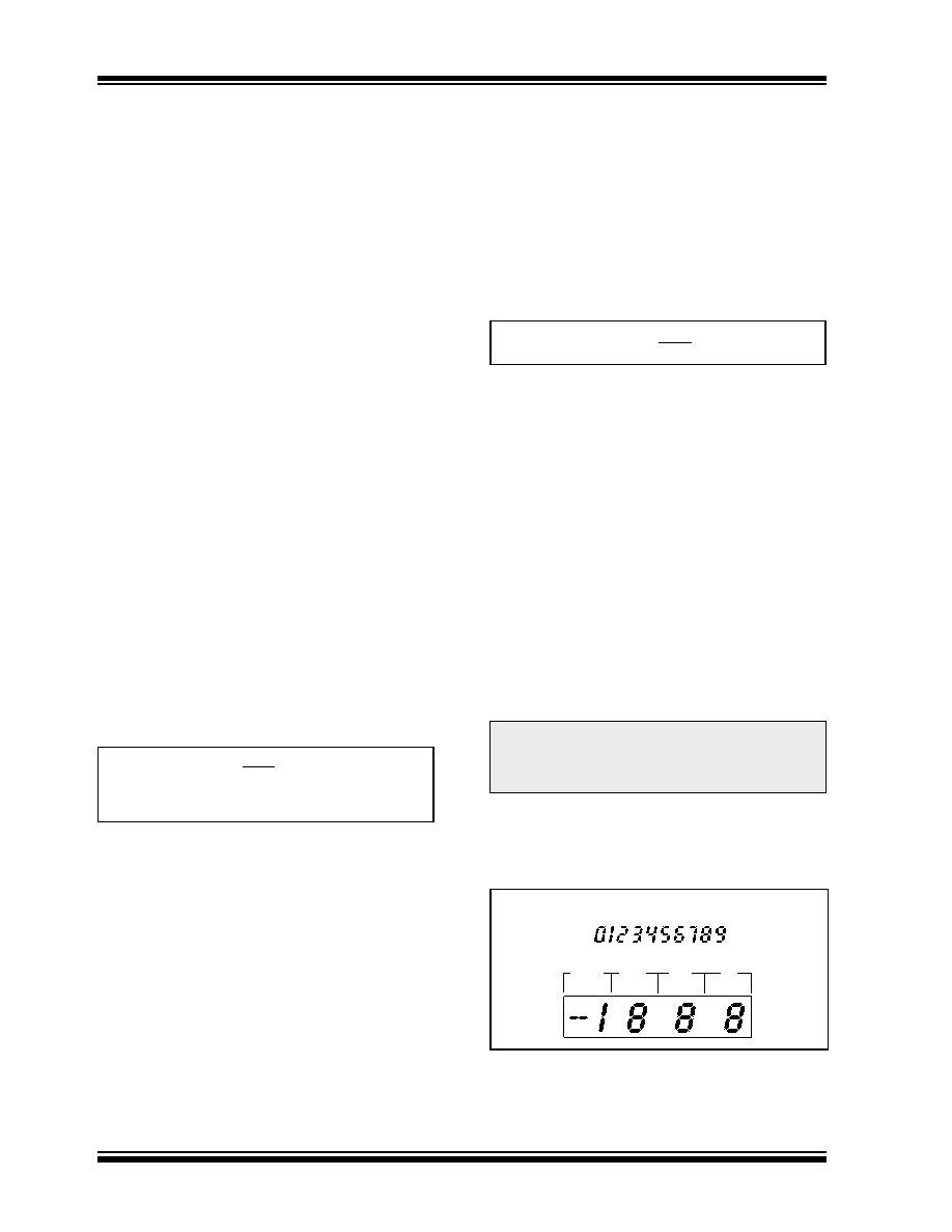
On the TC7126A, when the TEST pin is pulled to V+, all
segments are turned ON and the display reads -1888.
During this mode, LCD segments have a constant DC
voltage impressed.
The display font and segment drive assignment are
shownin Figure5-1.
FIGURE 5-1:
DISPLAY FONT AND
SEGMENT ASSIGNMENT
TSI =
4
FOSC
x 1000
Where: FOSC = external clock frequency.
Note:
Do not leave the display in this mode for
more than several minutes. LCDs may be
destroyed if operated with DC levels for
extended periods.
VIN
VREF
1000
Display Font
1000's
100's
10's
1's
相关PDF资料 |
PDF描述 |
|---|---|
| TC7126ACLW | 1-CH DUAL-SLOPE ADC, PQCC44 |
| TC7126CLW | 1-CH DUAL-SLOPE ADC, PQCC44 |
| TC7126CKW | 1-CH DUAL-SLOPE ADC, PQFP44 |
| TC7126ACLW713 | 1-CH DUAL-SLOPE ADC, PQCC44 |
| TC7126ACKW713 | 1-CH DUAL-SLOPE ADC, PQFP44 |
相关代理商/技术参数 |
参数描述 |
|---|---|
| TC7126RCPL | 功能描述:LCD 驱动器 Low Power RoHS:否 制造商:Maxim Integrated 数位数量:4.5 片段数量:30 最大时钟频率:19 KHz 工作电源电压:3 V to 3.6 V 最大工作温度:+ 85 C 最小工作温度:- 20 C 封装 / 箱体:PDIP-40 封装:Tube |
| TC7126RIPL | 制造商:MICROCHIP 制造商全称:Microchip Technology 功能描述:3-1/2 Digit Analog-to-Digital Converters |
| TC7129 | 制造商:MICROCHIP 制造商全称:Microchip Technology 功能描述:4-1/2 Digit Analog-to-Digital Converters with On-Chip LCD Drivers |
| TC7129_06 | 制造商:MICROCHIP 制造商全称:Microchip Technology 功能描述:4-1/2 Digit Analog-to-Digital Converters with On-Chip LCD Drivers |
| TC7129_13 | 制造商:MICROCHIP 制造商全称:Microchip Technology 功能描述:4-1/2 Digit Analog-to-Digital Converters with On-Chip LCD Drivers |
发布紧急采购,3分钟左右您将得到回复。