- 您现在的位置:买卖IC网 > PDF目录98179 > TC7135CKW 1-CH DUAL-SLOPE ADC, PQFP64 PDF资料下载
参数资料
| 型号: | TC7135CKW |
| 元件分类: | ADC |
| 英文描述: | 1-CH DUAL-SLOPE ADC, PQFP64 |
| 封装: | 10 X 10 MM, PLASTIC, MS-022, MQFP-44 |
| 文件页数: | 18/24页 |
| 文件大小: | 471K |
| 代理商: | TC7135CKW |
2004 Microchip Technology Inc.
DS21460C-page 3
TC7135
1.0
ELECTRICAL SPECIFICATIONS
Absolute Maximum Ratings
Positive Supply Voltage.....................................................+6V
Negative Supply Voltage ...................................................- 9V
Analog Input Voltage (Pin 9 or 10) ...............V+ to V- (Note 2)
Reference Input Voltage (Pin 2) ................................. V+ to V-
Clock Input Voltage ................................................... 0V to V+
Operating Temperature Range .......................... 0°C to +70°C
Storage Temperature Range ........................ –65°C to +150°C
Package Power Dissipation; (TA ≤ 70°C)
28-Pin PDIP .......................................................... 1.14
28-Pin PLCC ......................................................... 1.00
44-Pin MQFP
..........................................................................
64-Pin MQFP ........................................................ 1.14
Notice: Stresses above those listed under "Absolute Maxi-
mum Ratings" may cause permanent damage to the device.
These are stress ratings only and functional operation of the
device at these or any other conditions above those indicated
in the operation sections of the specifications is not implied.
Exposure to Absolute Maximum Rating conditions for
extended periods may affect device reliability.
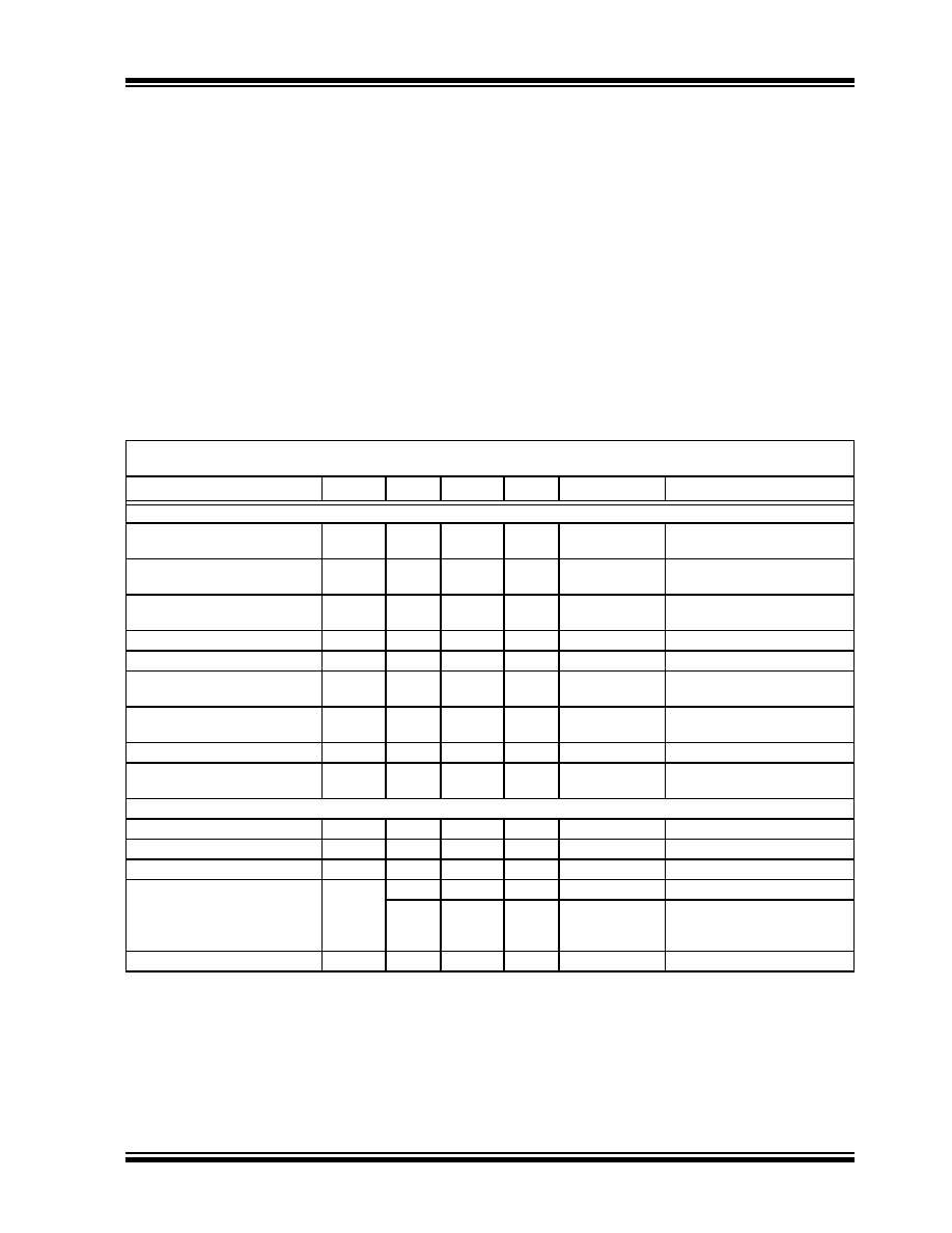
DC CHARACTERISTICS
Electrical Specifications: Unless otherwise indicated, TA = +25°C, FCLOCK = 120 kHz, V+ = +5V, V- = -5V.
(see Functional Block Diagram).
Parameters
Sym
Min.
Typ.
Max.
Units
Conditions
Analog
Display Reading with Zero Volt
Input
-0.0000
±0.0000
+0.0000
Display Reading
Zero Reading Temperature
Coefficient
TCZ
—0.5
2
V/°C
Full Scale Temperature
Coefficient
TCFS
—
5
ppm/°C
VIN = 2V,
Nonlinearity Error
NL
—
0.5
1
Count
Differential Linearity Error
DNL
—
0.01
—
LSB
Display Reading in Ratiometric
Operation
+0.9996
+0.9999
+1.0000
Display Reading
± Full Scale Symmetry Error
(Rollover Error)
±FSE
—
0.5
1
Count
Input Leakage Current
IIN
—
1
10
pA
Noise
eN
—15
—
VP-P
Peak-to-Peak Value not
Exceeded 95% of Time
Digital
Input Low Current
IIL
—
10
100
A
VIN = 0V
Input High Current
IIH
—0.08
10
A
VIN = +5V
Output Low Voltage
VOL
—
0.2
0.4
V
IOL = 1.6 mA
Output High Voltage;
B1, B2, B4, B8, D1 –D5
Busy, Polarity, Overrange,
Underrange, Strobe
VOH
2.4
4.4
5
V
IOH = 1 mA
4.9
4.99
5
V
IOH = 10 A
Clock Frequency
FCLK
0
200
1200
kHz
Note
1:
Limit input current to under 100 A if input voltages exceed supply voltage.
2:
Full-scale voltage = 2V
3:
VIN = 0V
4:
30°C
≤ T
A ≤ +70°C
5:
External reference temperature coefficient less than 0.01 ppm/°C.
6:
-2V
≤ V
IN ≤ +2V. Error of reading from best fit straight line.
7:
IVIN| = 1.9959
8:
Specification related to clock frequency range over which the
TC7135 correctly performs its various functions.
Increased errors result at higher operating frequencies.
相关PDF资料 |
PDF描述 |
|---|---|
| TC7135CLITR | 1-CH DUAL-SLOPE ADC, PQCC28 |
| TC7135CPI | 1-CH DUAL-SLOPE ADC, PDIP28 |
| TC7135CBU | 1-CH DUAL-SLOPE ADC, PQFP64 |
| TC7135CLI713 | 1-CH DUAL-SLOPE ADC, PQCC28 |
| TC7135CPIG | 1-CH DUAL-SLOPE ADC, PDIP28 |
相关代理商/技术参数 |
参数描述 |
|---|---|
| TC7135CLI | 功能描述:LED显示驱动器 4-1/2 Digit A/D BCD RoHS:否 制造商:Micrel 数位数量:5 片段数量: 安装风格:SMD/SMT 封装 / 箱体:PLCC-44 工作电源电压:4.75 V to 11 V 最大电源电流:10 mA 最大工作温度:+ 85 C 最小工作温度:- 40 C 封装:Tube |
| TC7135CLI713 | 功能描述:LED显示驱动器 4-1/2 Digit A/D BCD RoHS:否 制造商:Micrel 数位数量:5 片段数量: 安装风格:SMD/SMT 封装 / 箱体:PLCC-44 工作电源电压:4.75 V to 11 V 最大电源电流:10 mA 最大工作温度:+ 85 C 最小工作温度:- 40 C 封装:Tube |
| TC7135CPI | 功能描述:LED显示驱动器 4-1/2 Digit A/D BCD RoHS:否 制造商:Micrel 数位数量:5 片段数量: 安装风格:SMD/SMT 封装 / 箱体:PLCC-44 工作电源电压:4.75 V to 11 V 最大电源电流:10 mA 最大工作温度:+ 85 C 最小工作温度:- 40 C 封装:Tube |
| TC7135CPL | 制造商:MICROCHIP 制造商全称:Microchip Technology 功能描述:4-1/2 Digit A/D Converter |
| TC7136 | 制造商:MICROCHIP 制造商全称:Microchip Technology 功能描述:Low Power 3-1/2 Digit Analog-to-Digital Converter |
发布紧急采购,3分钟左右您将得到回复。