- 您现在的位置:买卖IC网 > PDF目录98179 > TC7136ACLW 1-CH DUAL-SLOPE ADC, ACCESS, PQCC44 PDF资料下载
参数资料
| 型号: | TC7136ACLW |
| 元件分类: | ADC |
| 英文描述: | 1-CH DUAL-SLOPE ADC, ACCESS, PQCC44 |
| 封装: | PLASTIC, LCC-44 |
| 文件页数: | 10/14页 |
| 文件大小: | 165K |
| 代理商: | TC7136ACLW |
5
LOW POWER, 3-1/2 DIGIT
ANALOG-TO-DIGITAL CONVERTERS
TC7136
TC7136A
GENERAL THEORY OF OPERATION
(All Pin designations refer to 40-Pin Dip)
Dual-Slope Conversion Principles
The TC7136/A is a dual-slope, integrating analog-to-
digital converter. An understanding of the dual-slope con-
version technique will aid in following detailed TC7136/A
operational theory.
The conventional dual-slope converter measurement
cycle has two distinct phases:
(1) Input signal integration
(2) Reference voltage integration (deintegration)
The input signal being converted is integrated for a fixed
time period (tSI), measured by counting clock pulses. An
opposite polarity constant reference voltage is then inte-
grated until the integrator output voltage returns to zero. The
reference integration time is directly proportional to the input
signal (tRI).
In a simple dual-slope converter, a complete conversion
requires the integrator output to "ramp-up" and "ramp-
down."
A simple mathematical equation relates the input signal,
reference voltage, and integration time:
TC7136/A PIN DESCRIPTION (Cont.)
Pin No.
40-Pin PDIP
Normal
(Reverse)
Name
Description
33
(8)
C
–
REF
See pin 34.
34
(7)
C
+
REF
A 0.1
F capacitor is used in most applications. If a large common-mode
voltage exists (for example, the V
–
IN pin is not at analog common), and a 200
mV scale is used, a 1
F capacitor is recommended and will hold the roll-over
error to 0.5 count.
35
(6)
V
–
REF
See pin 36.
(5)
V
+
REF
The analog input required to generate a full-scale output (1999 counts). Place
100 mV between pins 35 and 36 for 199.9 mV full scale. Place 1V between
pins 35 and 36 for 2V full scale. See paragraph on Reference Voltage.
36
(4)
TEST
Lamp test. When pulled HIGH (to V+) all segments will be turned ON and the
display should read –1888. It may also be used as a negative supply for exter-
nally-generated decimal points. See paragraph under Test for additional informa-
tion.
37
(3)
OSC3
See pin 40.
38
(2)
OSC2
See pin 40.
39
(1)
OSC1
Pins 40, 39 and 38 make up the oscillator section. For a 48kHz clock (3 readings per
second) connect pin 40 to the junction of a 180 k
resistor and a 50pF capacitor. The
180k
resistor is tied to pin 39 and the 50pF capacitor is tied to pin 38.
For a constant VIN:
VIN = VR
.
1VR tRI
RC
VIN(t) dt =
,
tSI
where:
VR = Reference voltage
tSI = Signal integration time (fixed)
tRI = Reference voltage integration time (variable).
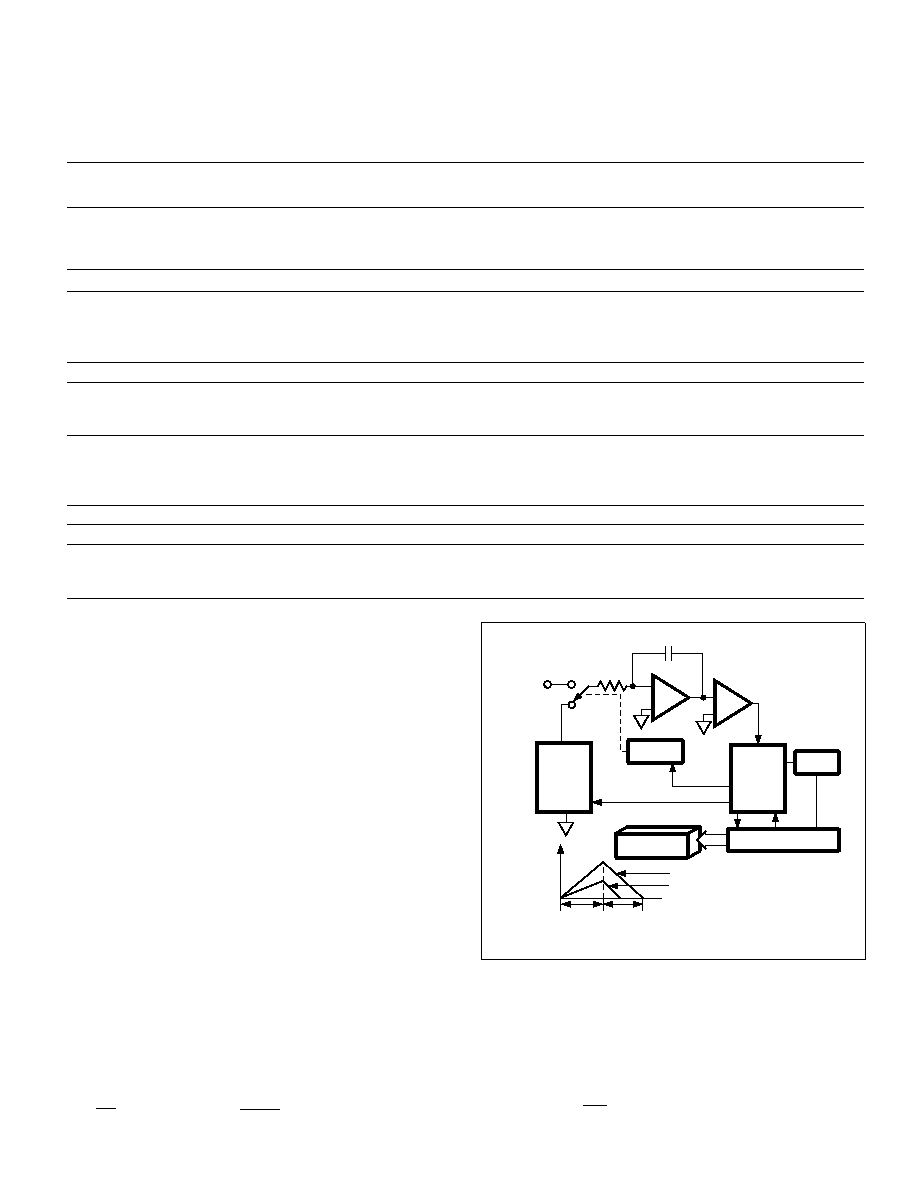
Figure 1. Basic Dual-Slope Converter
+
–
REF
VOLTAGE
ANALOG
INPUT
SIGNAL
+
–
DISPLAY
SWITCH
DRIVER
CONTROL
LOGIC
INTEGRATOR
OUTPUT
CLOCK
COUNTER
POLARITY CONTROL
PHASE
CONTROL
VIN
VFULL SCALE
1.2 VFULL SCALE
VARIABLE
REFERENCE
INTEGRATE
TIME
FIXED
SIGNAL
INTEGRATE
TIME
INTEGRATOR
CINT
COMPARATOR
tRI
tSI
[ ]
0
∫
相关PDF资料 |
PDF描述 |
|---|---|
| TC7136CLW | 1-CH DUAL-SLOPE ADC, ACCESS, PQCC44 |
| TC7136ACKW | 1-CH DUAL-SLOPE ADC, ACCESS, PQFP44 |
| TC7136CKW | 1-CH DUAL-SLOPE ADC, ACCESS, PQFP44 |
| TC7136ACLW | 1-CH DUAL-SLOPE ADC, PQCC44 |
| TC7136ACPI | 1-CH DUAL-SLOPE ADC, PDIP40 |
相关代理商/技术参数 |
参数描述 |
|---|---|
| TC7136ACLW713 | 功能描述:LCD 驱动器 Low Power RoHS:否 制造商:Maxim Integrated 数位数量:4.5 片段数量:30 最大时钟频率:19 KHz 工作电源电压:3 V to 3.6 V 最大工作温度:+ 85 C 最小工作温度:- 20 C 封装 / 箱体:PDIP-40 封装:Tube |
| TC7136ACPI | 制造商:MICROCHIP 制造商全称:Microchip Technology 功能描述:Low Power 3-1/2 Digit Analog-to-Digital Converter |
| TC7136ACPL | 功能描述:LCD 驱动器 Low Power RoHS:否 制造商:Maxim Integrated 数位数量:4.5 片段数量:30 最大时钟频率:19 KHz 工作电源电压:3 V to 3.6 V 最大工作温度:+ 85 C 最小工作温度:- 20 C 封装 / 箱体:PDIP-40 封装:Tube |
| TC7136ARCPL | 功能描述:LCD 驱动器 Low Power RoHS:否 制造商:Maxim Integrated 数位数量:4.5 片段数量:30 最大时钟频率:19 KHz 工作电源电压:3 V to 3.6 V 最大工作温度:+ 85 C 最小工作温度:- 20 C 封装 / 箱体:PDIP-40 封装:Tube |
| TC7136CKW | 功能描述:LCD 驱动器 Low Power RoHS:否 制造商:Maxim Integrated 数位数量:4.5 片段数量:30 最大时钟频率:19 KHz 工作电源电压:3 V to 3.6 V 最大工作温度:+ 85 C 最小工作温度:- 20 C 封装 / 箱体:PDIP-40 封装:Tube |
发布紧急采购,3分钟左右您将得到回复。