- 您现在的位置:买卖IC网 > PDF目录98179 > TC7136ACLW 1-CH DUAL-SLOPE ADC, PQCC44 PDF资料下载
参数资料
| 型号: | TC7136ACLW |
| 元件分类: | ADC |
| 英文描述: | 1-CH DUAL-SLOPE ADC, PQCC44 |
| 封装: | PLASTIC, LCC-44 |
| 文件页数: | 2/22页 |
| 文件大小: | 410K |
| 代理商: | TC7136ACLW |
TC7136/TC7136A
DS21461C-page 10
2005 Microchip Technology Inc.
4.0
ANALOG SECTION
In addition to the basic integrate and de-integrate dual
slope cycles discussed above, the TC7136 and
TC7136A designs incorporate an "integrator output
zero cycle" and an "auto-zero cycle." These additional
cycles ensure the integrator starts at 0V (even after a
severe over range conversion) and that all offset volt-
age errors (buffer amplifier, integrator and comparator)
are removed from the conversion. A true digital zero
reading is assured without any external adjustments.
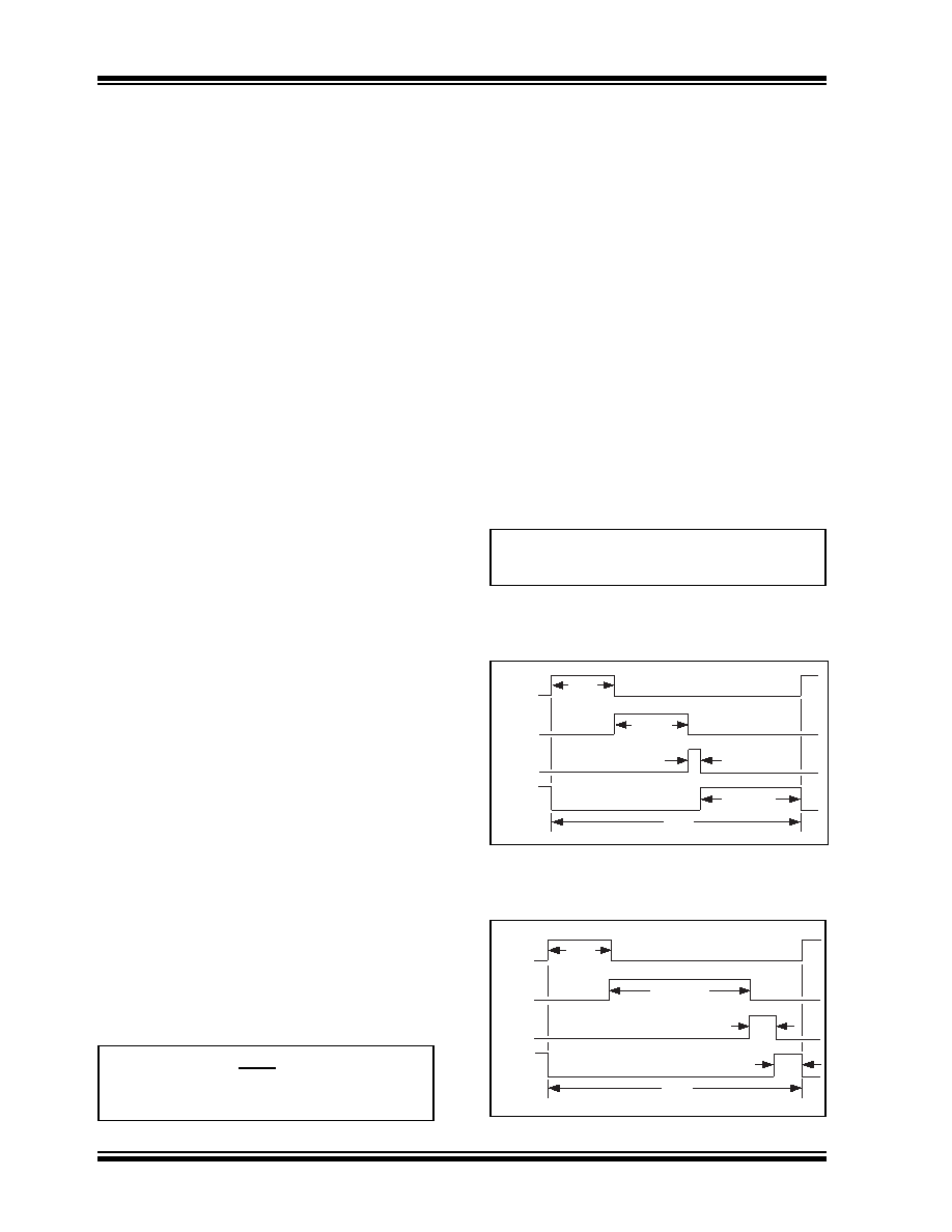
A complete conversion consists of four distinct phases:
1.
Integrator output zero phase
2.
Auto-zero phase
3.
Signal integrate phase
4.
Reference de-integrate phase
4.1
Integrator Output Zero Phase
This phase ensures the integrator output is at 0V
before the system zero phase is entered. This ensures
that true system offset voltages will be compensated
for, even after an over range conversion. The count for
this phase is a function of the number of counts
required by the de-integrate phase. The count lasts
from 11 to 140 counts for non over range conversions
and from 31 to 640 counts for over range conversions.
4.2
Auto-Zero Phase
During the auto-zero phase, the differential input signal
is disconnected from the circuit by opening internal
analog gates. The internal nodes are shorted to analog
common (ground) to establish a zero input condition.
Additional analog gates close a feedback loop around
the integrator and comparator. This loop permits com-
parator offset voltage error compensation. The voltage
level established on CAZ compensates for device offset
voltages. The auto-zero phase residual is typically
10
μV to 15μV.
The auto-zero duration is from 910 to 2900 counts for
non over range conversions and from 300 to 910
counts for over range conversions.
4.3
Signal Integration Phase
The auto-zero loop is entered and the internal differen-
tial inputs connect to VIN+ and VIN-. The differential
input signal is integrated for a fixed time period. The
TC7136/A signal integration period is 1000 clock peri-
ods or counts. The externally set clock frequency is
divided by four before clocking the internal counters.
The integration time period is:
EQUATION 4-1:
The differential input voltage must be within the device
Common mode range when the converter and mea-
sured system share the same power supply common
(ground). If the converter and measured system do not
share the same power supply common, VIN- should be
tied to analog common.
Polarity is determined at the end of signal integrate
phase. The sign bit is a true polarity indication, in that
signals less than 1LSB are correctly determined. This
allows precision null detection, limited only by device
noise and auto-zero residual offsets.
4.4
Reference Integrate Phase
The third phase is reference integrate or de-integrate.
VIN- is internally connected to analog common and
VIN+ is connected across the previously charged refer-
ence capacitor. Circuitry within the chip ensures that
the capacitor will be connected with the correct polarity
to cause the integrator output to return to zero. The
time required for the output to return to zero is propor-
tional to the input signal and is between 0 and 2000
internal clock periods. The digital reading displayed is:
EQUATION 4-2:
FIGURE 4-1:
CONVERSION TIMING
DURING NORMAL
OPERATION
FIGURE 4-2:
CONVERSION TIMING
DURING OVER RANGE
OPERATION
tSI =
x 1000
4
FOSC
Where FOSC = external clock frequency.
1000
V
IN
V
REF
----------------
=
INT
DENT
ZI
AZ
4000
910-2900
1-2000
1000
11-140
AZ
4000
ZI
DEINT
INT
1000
2001-2090
31-640
300-910
相关PDF资料 |
PDF描述 |
|---|---|
| TC7136ACPI | 1-CH DUAL-SLOPE ADC, PDIP40 |
| TC7136CLW | 1-CH DUAL-SLOPE ADC, PQCC44 |
| TC7136CLW713 | 1-CH DUAL-SLOPE ADC, PQCC44 |
| TC7136ACLW713 | 1-CH DUAL-SLOPE ADC, PQCC44 |
| TC7136ACKW | 1-CH DUAL-SLOPE ADC, PQFP44 |
相关代理商/技术参数 |
参数描述 |
|---|---|
| TC7136ACLW713 | 功能描述:LCD 驱动器 Low Power RoHS:否 制造商:Maxim Integrated 数位数量:4.5 片段数量:30 最大时钟频率:19 KHz 工作电源电压:3 V to 3.6 V 最大工作温度:+ 85 C 最小工作温度:- 20 C 封装 / 箱体:PDIP-40 封装:Tube |
| TC7136ACPI | 制造商:MICROCHIP 制造商全称:Microchip Technology 功能描述:Low Power 3-1/2 Digit Analog-to-Digital Converter |
| TC7136ACPL | 功能描述:LCD 驱动器 Low Power RoHS:否 制造商:Maxim Integrated 数位数量:4.5 片段数量:30 最大时钟频率:19 KHz 工作电源电压:3 V to 3.6 V 最大工作温度:+ 85 C 最小工作温度:- 20 C 封装 / 箱体:PDIP-40 封装:Tube |
| TC7136ARCPL | 功能描述:LCD 驱动器 Low Power RoHS:否 制造商:Maxim Integrated 数位数量:4.5 片段数量:30 最大时钟频率:19 KHz 工作电源电压:3 V to 3.6 V 最大工作温度:+ 85 C 最小工作温度:- 20 C 封装 / 箱体:PDIP-40 封装:Tube |
| TC7136CKW | 功能描述:LCD 驱动器 Low Power RoHS:否 制造商:Maxim Integrated 数位数量:4.5 片段数量:30 最大时钟频率:19 KHz 工作电源电压:3 V to 3.6 V 最大工作温度:+ 85 C 最小工作温度:- 20 C 封装 / 箱体:PDIP-40 封装:Tube |
发布紧急采购,3分钟左右您将得到回复。