参数资料
| 型号: | TC7650CPD |
| 厂商: | Microchip Technology |
| 文件页数: | 11/14页 |
| 文件大小: | 0K |
| 描述: | IC OPAMP CHOPPER STAB 14DIP |
| 标准包装: | 30 |
| 放大器类型: | 断路器(零漂移) |
| 电路数: | 1 |
| 转换速率: | 2.5 V/µs |
| 增益带宽积: | 2MHz |
| 电流 - 输入偏压: | 1.5pA |
| 电压 - 输入偏移: | 0.7µV |
| 电流 - 电源: | 2mA |
| 电压 - 电源,单路/双路(±): | 4.5 V ~ 16 V,±2.25 V ~ 8 V |
| 工作温度: | 0°C ~ 70°C |
| 安装类型: | 通孔 |
| 封装/外壳: | 14-DIP(0.300",7.62mm) |
| 供应商设备封装: | 14-PDIP |
| 包装: | 管件 |
| 产品目录页面: | 680 (CN2011-ZH PDF) |
TC7650
DS21463B-page 6
2002 Microchip Technology Inc.
positive duty cycle is desired for frequencies above
500Hz to ensure transients settle before the internal
switches open.
The external clock input can also be used as a strobe
input. If a strobe signal is connected at the external
clock input so that it is LOW during the time an overload
signal is applied, neither capacitor will be charged. The
leakage currents at the capacitors pins are very low. At
25°C a typical TC7650 will drift less than 10
V/sec.
3.6
Output Clamp
Chopper-stabilized systems can show long recovery
times from overloads. If the output is driven to either
supply rail, output saturation occurs. The inputs are no
longer held at a "virtual ground." The VOS null circuit
treats the differential signal as an offset and tries to cor-
rect it by charging the external capacitors. The nulling
circuit also saturates. Once the input signal returns to
normal, the response time is lengthened by the long
recovery time of the nulling amplifier and external
capacitors.
Through an external clamp connection, the TC7650
eliminates the overload recovery problem by reducing
the feedback network gain before the output voltage
reaches either supply rail.
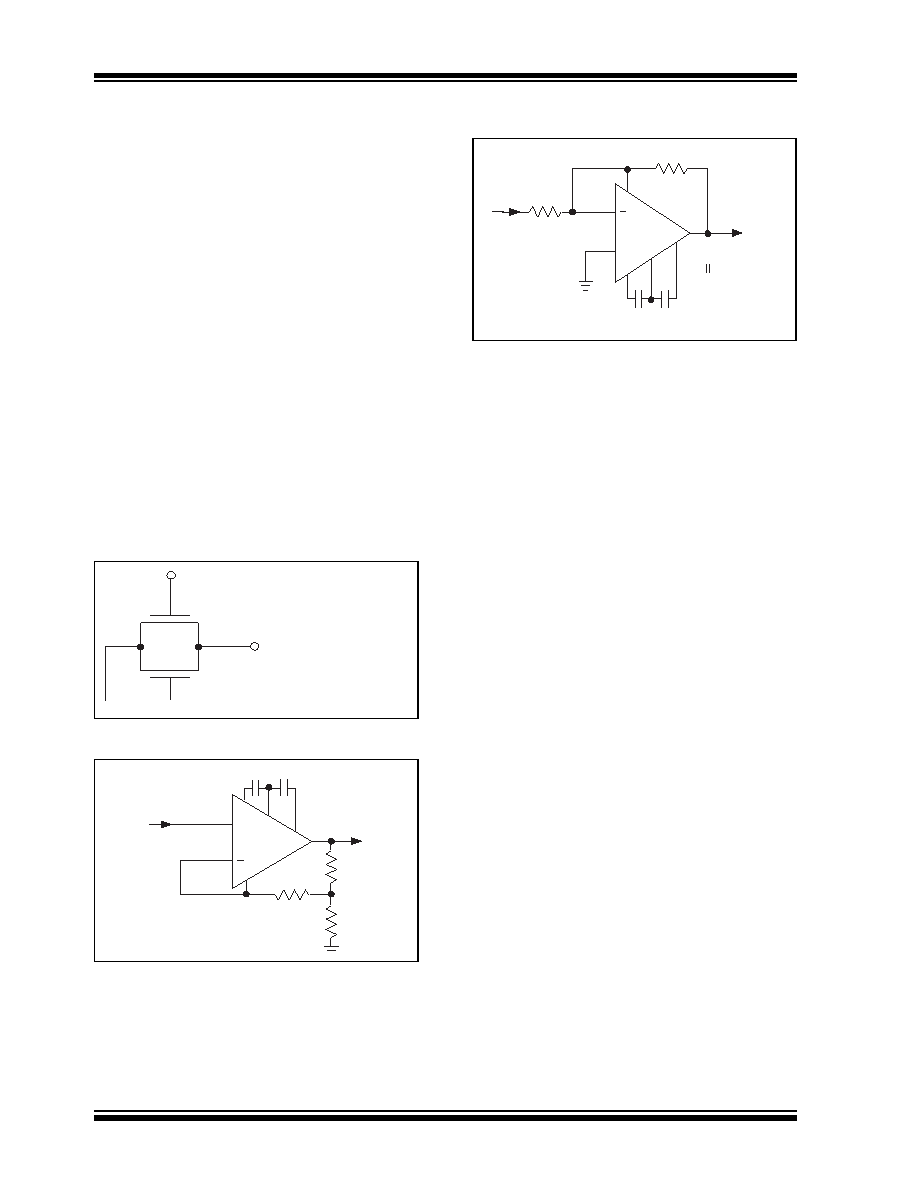
FIGURE 3-3:
INTERNAL CLAMP CIRCUIT
FIGURE 3-4:
NON-INVERTING AMPLIFIER
WITH OPTIONAL CLAMP
FIGURE 3-5:
INVERTING AMPLIFIER WITH
OPTIONAL CLAMP
The output clamp circuit is shown in Figure 3-3, with
typical inverting and non-inverting circuit connections
shown in Figures 3-4 and 3-5. Output voltage versus
clamp circuit current characteristics are shown in the
typical operating curves. For the clamp to be fully effec-
tive, the impedance across the clamp output should be
greater than 100k
.
3.7
Latch-Up Avoidance
Junction-isolated CMOS circuits inherently include a
parasitic 4-layer (p-n-p-n) structure which has charac-
teristics similar to an SCR. Under certain circum-
stances this junction may be triggered into a low-
impedance state, resulting in excessive supply current.
To avoid this condition, no voltage greater than 0.3V
beyond the supply rails should be applied to any pin. In
general, the amplifier supplies must be established
either at the same time or before any input signals are
applied. If this is not possible, the drive circuits must
limit input current flow to under 0.1mA to avoid latch-
up.
3.8
Thermoelectric Potentials
Precision DC measurements are ultimately limited by
thermoelectric potentials developed in thermocouple
junctions of dissimilar metals, alloys, silicon, etc.
Unless all junctions are at the same temperature, ther-
moelectric voltages, typically around 0.1
V/°C, but up
to tens of
V/°C for some materials, will be generated.
In order to realize the benefits extremely-low offset volt-
ages provide, it is essential to take special precautions
to avoid temperature gradients. All components should
be enclosed to eliminate air movement, especially
those caused by power dissipating elements in the sys-
tem.
Low
thermoelectric
co-efficient
connections
should be used where possible and power supply volt-
ages and power dissipation should be kept to a mini-
mum. High impedance loads are preferable, and
separation from surrounding heat dissipating elements
is advised.
Internal
Positive Clamp Bias
≈ V+ - VT ≈ V+ - 0.7
P-Channel
Output
Clamp Pin
N-Channel
TC7650
+
C
R
C
Output
Input
For Full Clamp Effect
R2
R1
R3 + (R1/R2) 100 k
0.1F
Connect To VSS
On 8-Pin DIP.
*
R
Clamp
3
TC7650
Clamp
+
C
R
C
R1
Output
0.1 F
0.1 F
Input
R2
For Full Clamp
Effect
*
Connect To VR
On 8-Pin DIP.
*
–
(R1 R2) 100 k
相关PDF资料 |
PDF描述 |
|---|---|
| TC7652CPD | IC OPAMP CHOPPER STAB LN 14DIP |
| TC913ACPA | IC OPAMP DUAL AUTO ZERO 8DIP |
| TCA0372DWG | IC OPAMP DUAL POWER 1A 16SOIC |
| TDA1348AE | 48V FAN 127X127X38MM |
| TDA1548AG | 48V FAN 172X150X50.8MM |
相关代理商/技术参数 |
参数描述 |
|---|---|
| TC7650IJA | 功能描述:运算放大器 - 运放 Low VOS CMOS RoHS:否 制造商:STMicroelectronics 通道数量:4 共模抑制比(最小值):63 dB 输入补偿电压:1 mV 输入偏流(最大值):10 pA 工作电源电压:2.7 V to 5.5 V 安装风格:SMD/SMT 封装 / 箱体:QFN-16 转换速度:0.89 V/us 关闭:No 输出电流:55 mA 最大工作温度:+ 125 C 封装:Reel |
| TC7650IJD | 功能描述:运算放大器 - 运放 Low VOS CMOS RoHS:否 制造商:STMicroelectronics 通道数量:4 共模抑制比(最小值):63 dB 输入补偿电压:1 mV 输入偏流(最大值):10 pA 工作电源电压:2.7 V to 5.5 V 安装风格:SMD/SMT 封装 / 箱体:QFN-16 转换速度:0.89 V/us 关闭:No 输出电流:55 mA 最大工作温度:+ 125 C 封装:Reel |
| TC7652 | 制造商:MICROCHIP 制造商全称:Microchip Technology 功能描述:Low Noise, Chopper Stabilized Operational Amplifier |
| TC7652_13 | 制造商:MICROCHIP 制造商全称:Microchip Technology 功能描述:Low Noise, Chopper Stabilized Operational Amplifier |
| TC7652CPA | 功能描述:运算放大器 - 运放 Low Noise Op Amp RoHS:否 制造商:STMicroelectronics 通道数量:4 共模抑制比(最小值):63 dB 输入补偿电压:1 mV 输入偏流(最大值):10 pA 工作电源电压:2.7 V to 5.5 V 安装风格:SMD/SMT 封装 / 箱体:QFN-16 转换速度:0.89 V/us 关闭:No 输出电流:55 mA 最大工作温度:+ 125 C 封装:Reel |
发布紧急采购,3分钟左右您将得到回复。