- 您现在的位置:买卖IC网 > PDF目录299959 > TC7652CPDG OP-AMP, 5000 uV OFFSET-MAX, 0.4 MHz BAND WIDTH, PDIP14 PDF资料下载
参数资料
| 型号: | TC7652CPDG |
| 元件分类: | 运算放大器 |
| 英文描述: | OP-AMP, 5000 uV OFFSET-MAX, 0.4 MHz BAND WIDTH, PDIP14 |
| 封装: | PLASTIC, DIP-14 |
| 文件页数: | 10/16页 |
| 文件大小: | 456K |
| 代理商: | TC7652CPDG |
2002 Microchip Technology Inc.
DS21464B-page 3
TC7652
1.0
ELECTRICAL
CHARACTERISTICS
ABSOLUTE MAXIMUM RATINGS*
Total Supply Voltage (VDD to VSS) .......................+18V
Input Voltage .................... (VDD +0.3V) to (VSS –0.3V)
Voltage on Oscillator Control Pins...............VDD to VSS
Duration of Output Short Circuit ..................... Indefinite
Current Into Any Pin............................................ 10mA
WhileOperating(Note 1)............................ 100
A
Package Power Dissipation (TA < 70°C)
8-Pin Plastic DIP ....................................... 730mW
14-Pin Plastic DIP ..................................... 800mW
Storage Temperature Range .............. -65°C to +150°C
Operating Temperature Range
C Device .......................................... 0°C to +70°C
I Device ......................................... -25°C to +85°C
*Stresses above those listed under “Absolute Maximum
Ratings” may cause permanent damage to the device.
These are stress ratings only and functional operation of the
device at these or any other conditions above those indi-
cated in the operation sections of the specifications is not
implied. Exposure to Absolute Maximum Rating conditions
for extended periods my affect device reliability.
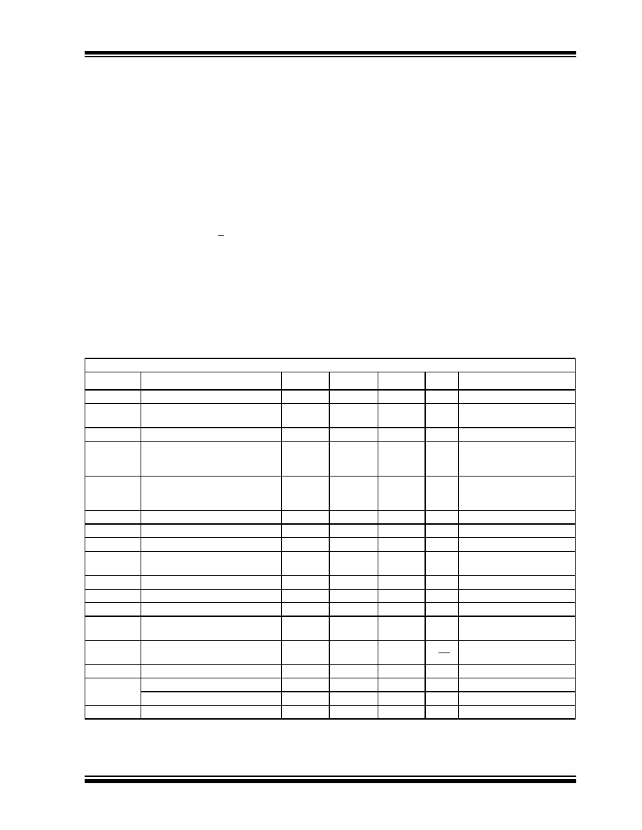
TC7652 ELECTRICAL SPECIFICATIONS
Electrical Characteristics: VDD =+5V,VSS =-5V, TA = +25°C, unless otherwise indicated.
Symbol
Parameter
Min
Typ
Max
Units
Test Conditions
VOS
Input Offset Voltage
—
±2
±5
VTA =+25°C
TCVOS
Average Temperature Co-efficient of
Input Offset Voltage
—0.01
0.05
V/°C 0°C < TA <+70°C
VOS/DT
Offset Voltage vs Time
—
150
—
nV/mo
IBIAS
Input Bias Current (CLK On)
—
30
100
250
100
—
1000
pA
TA =+25°C
0°C < TA <+70°C
-25°C < TA <+85°C
IBIAS
Input Bias Current (CLK Off)
—
15
35
100
30
—
1000
pA
TA =+25°C
0°C < TA <+70°C
-25°C < TA <+85°C
IOS
Input Offset Current
—
25
150
pA
RIN
Input Resistance
—
1012
—
OL
Large Signal Voltage Gain
120
150
—
dB
RL =10k,VOUT =±4V
VOUT
Output Voltage Swing (Note 2)±4.7
—
±4.85
±4.95
—
VRL =10k
RL = 100k
CMVR
Common Mode Voltage Range
-4.3
—
+3.5
V
MRR
Common Mode Rejection Ratio
120
140
—
dB
CMVR = -4.3V to +3.5V
PSRR
Power Supply
120
140
—
dB
±3V to ±8V
eN
Input Noise Voltage
—
0.2
0.7
1.5
5
VP-P
RS =100,DC to 1Hz
DC to 10Hz
IN
Input Noise Current
—
0.01
—
pA/
√Hz
f =10Hz
GBW
Unity Gain Bandwidth
—
0.4
—
MHz
SR
Slew Rate
—
1
—
V/
sec CL = 50pF, RL =10k
Overshoot
—
15
—
%
VDD,VSS
Operating Supply Range
5
—
16
V
Note
1:
Limiting input current to 100
A is recommended to avoid latch-up problems. Typically 1mA is safe however, this is not
guaranteed.
2:
Output clamp not connected. See typical characteristics curves for output swing versus clamp current characteristics.
3:
See “Output Clamp” under detailed description.
相关PDF资料 |
PDF描述 |
|---|---|
| TC8-ED7754/4 | 0.5 MHz - 300 MHz RF TRANSFORMER |
| TCBZX55C10.TR | 10 V, 0.5 W, SILICON, UNIDIRECTIONAL VOLTAGE REGULATOR DIODE, DO-35 |
| TCBZX55C6V2 | 6.2 V, 0.5 W, SILICON, UNIDIRECTIONAL VOLTAGE REGULATOR DIODE, DO-35 |
| TCBZX79C24.TR | 24.2 V, 0.5 W, SILICON, UNIDIRECTIONAL VOLTAGE REGULATOR DIODE, DO-35 |
| TCBZX79C8V2 | 8.2 V, 0.5 W, SILICON, UNIDIRECTIONAL VOLTAGE REGULATOR DIODE, DO-35 |
相关代理商/技术参数 |
参数描述 |
|---|---|
| TC7652IJA | 功能描述:运算放大器 - 运放 Low Noise RoHS:否 制造商:STMicroelectronics 通道数量:4 共模抑制比(最小值):63 dB 输入补偿电压:1 mV 输入偏流(最大值):10 pA 工作电源电压:2.7 V to 5.5 V 安装风格:SMD/SMT 封装 / 箱体:QFN-16 转换速度:0.89 V/us 关闭:No 输出电流:55 mA 最大工作温度:+ 125 C 封装:Reel |
| TC7652IJD | 功能描述:运算放大器 - 运放 Low Noise RoHS:否 制造商:STMicroelectronics 通道数量:4 共模抑制比(最小值):63 dB 输入补偿电压:1 mV 输入偏流(最大值):10 pA 工作电源电压:2.7 V to 5.5 V 安装风格:SMD/SMT 封装 / 箱体:QFN-16 转换速度:0.89 V/us 关闭:No 输出电流:55 mA 最大工作温度:+ 125 C 封装:Reel |
| TC7660 | 制造商:MICRO CHIP 功能描述: |
| TC7660_02 | 制造商:MICROCHIP 制造商全称:Microchip Technology 功能描述:Charge Pump DC-to-DC Voltage Converter |
| TC7660CJA | 制造商:MICROCHIP 制造商全称:Microchip Technology 功能描述:Charge Pump DC-to-DC Voltage Converter |
发布紧急采购,3分钟左右您将得到回复。