- 您现在的位置:买卖IC网 > PDF目录69482 > TC7660CPA SWITCHED CAPACITOR REGULATOR, 10 kHz SWITCHING FREQ-MAX, PDIP8 PDF资料下载
参数资料
| 型号: | TC7660CPA |
| 元件分类: | 稳压器 |
| 英文描述: | SWITCHED CAPACITOR REGULATOR, 10 kHz SWITCHING FREQ-MAX, PDIP8 |
| 封装: | PLASTIC, DIP-8 |
| 文件页数: | 15/18页 |
| 文件大小: | 396K |
| 代理商: | TC7660CPA |
TC7660
DS21465B-page 6
2002 Microchip Technology Inc.
4.0
DETAILED DESCRIPTION
4.1
Theory of Operation
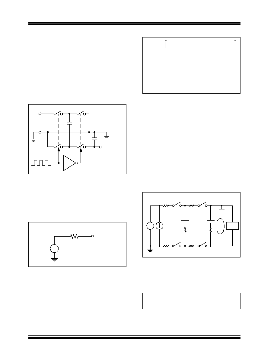
The TC7660 charge pump converter inverts the voltage
applied to the V + pin. The conversion consists of a two-
phase operation (Figure 4-1). During the first phase,
switches S2 and S4 are open and switches S1 and S3
are closed. C1 charges to the voltage applied to the V
+
pin, with the load current being supplied from C2. Dur-
ing the second phase, switches S2 and S4 are closed
and switches S1 and S3 are open. Charge is trans-
ferred from C1 to C2, with the load current being
supplied from C1.
FIGURE 4-1:
Ideal Switched Capacitor
Inverter.
In this manner, the TC7660 performs a voltage inver-
sion, but does not provide regulation. The average out-
put voltage will drop in a linear manner with respect to
load current. The equivalent circuit of the charge pump
inverter can be modeled as an ideal voltage source in
series with a resistor, as shown in Figure 4-2.
FIGURE 4-2:
Switched Capacitor Inverter
Equivalent Circuit Model.
The value of the series resistor (ROUT) is a function of
the switching frequency, capacitance and equivalent
series resistance (ESR) of C1 and C2 and the on-resis-
tance of switches S1, S2, S3 and S4. A close
approximation for ROUT is given in the following
equation:
EQUATION
4.2
Switched Capacitor Inverter
Power Losses
The overall power loss of a switched capacitor inverter
is affected by four factors:
1.
Losses from power consumed by the internal
oscillator, switch drive, etc. These losses will
vary with input voltage, temperature and
oscillator frequency.
2.
Conduction losses in the non-ideal switches.
3.
Losses due to the non-ideal nature of the
external capacitors.
4.
Losses that occur during charge transfer from
C1 to C2 when a voltage difference between the
capacitors exists.
Figure 4-3 depicts the non-ideal elements associated
with the switched capacitor inverter power loss.
FIGURE 4-3:
Non-Ideal Switched
Capacitor Inverter.
The power loss is calculated using the following
equation:
EQUATION
V+
GND S
3
S1
S2
S4
C2
VOUT = -VIN
C1
+
-
+
ROUT
VOUT
V+
ROUT
1
fPUMP C1
×
----------------------------- 8R
SW
4ESRC1 ESRC2
++
+
=
RSW
on-resistance of the switches
=
ESRC1
equivalent series resistance of C1
=
ESRC2
equivalent series resistance of C2
=
fPUMP
fOSC
2
-----------
=
Where:
LOAD
C1
C2
RSW
S1
IDD
ESRC1
V+
+
-
RSW
S2
RSW
S3
RSW
S4
ESRC2
IOUT
++
PLOSS
IOUT
2
ROUT
×
IDD V
+
×
+
=
相关PDF资料 |
PDF描述 |
|---|---|
| TC7660EOAG | SWITCHED CAPACITOR REGULATOR, 10 kHz SWITCHING FREQ-MAX, PDSO8 |
| TC7660MJA | SWITCHED CAPACITOR REGULATOR, CDIP8 |
| TC7660COA | SWITCHED CAPACITOR REGULATOR, PDSO8 |
| TC7660EPA | SWITCHED CAPACITOR REGULATOR, PDIP8 |
| TC7660SEPA | SWITCHED CAPACITOR REGULATOR, 45 kHz SWITCHING FREQ-MAX, PDIP8 |
相关代理商/技术参数 |
参数描述 |
|---|---|
| TC7660CPA | 制造商:TELCOM SEMICONDUCTOR 功能描述:IC VOLT CONVERTER 7660 DIP8 |
| TC7660CPA | 制造商:Microchip Technology Inc 功能描述:DC-DC Converter |
| TC7660EJA | 制造商:MICROCHIP 制造商全称:Microchip Technology 功能描述:Charge Pump DC-to-DC Voltage Converter |
| TC7660EOA | 功能描述:电荷泵 DC-DC Converter RoHS:否 制造商:Maxim Integrated 功能:Inverting, Step Up 输出电压:- 1.5 V to - 5.5 V, 3 V to 11 V 输出电流:100 mA 电源电流:1 mA 最大工作温度:+ 70 C 封装 / 箱体:SOIC-8 Narrow 封装:Tube |
| TC7660EOA | 制造商:Microchip Technology Inc 功能描述:ICS POWER SUPPLY PACKAGE/CASE:8-SOIC |
发布紧急采购,3分钟左右您将得到回复。