- 您现在的位置:买卖IC网 > PDF目录69482 > TC7MPB9327FTG DUAL 1-CHANNEL, SGL POLE DOUBLE THROW SWITCH, PQCC16 PDF资料下载
参数资料
| 型号: | TC7MPB9327FTG |
| 元件分类: | 多路复用及模拟开关 |
| 英文描述: | DUAL 1-CHANNEL, SGL POLE DOUBLE THROW SWITCH, PQCC16 |
| 封装: | 3 X 3 MM, 0.50 MM PITCH, PLASTIC, VQON-16 |
| 文件页数: | 11/14页 |
| 文件大小: | 336K |
| 代理商: | TC7MPB9327FTG |
TC7MPB9326,9327FT/FK/FTG
2009-09-11
6
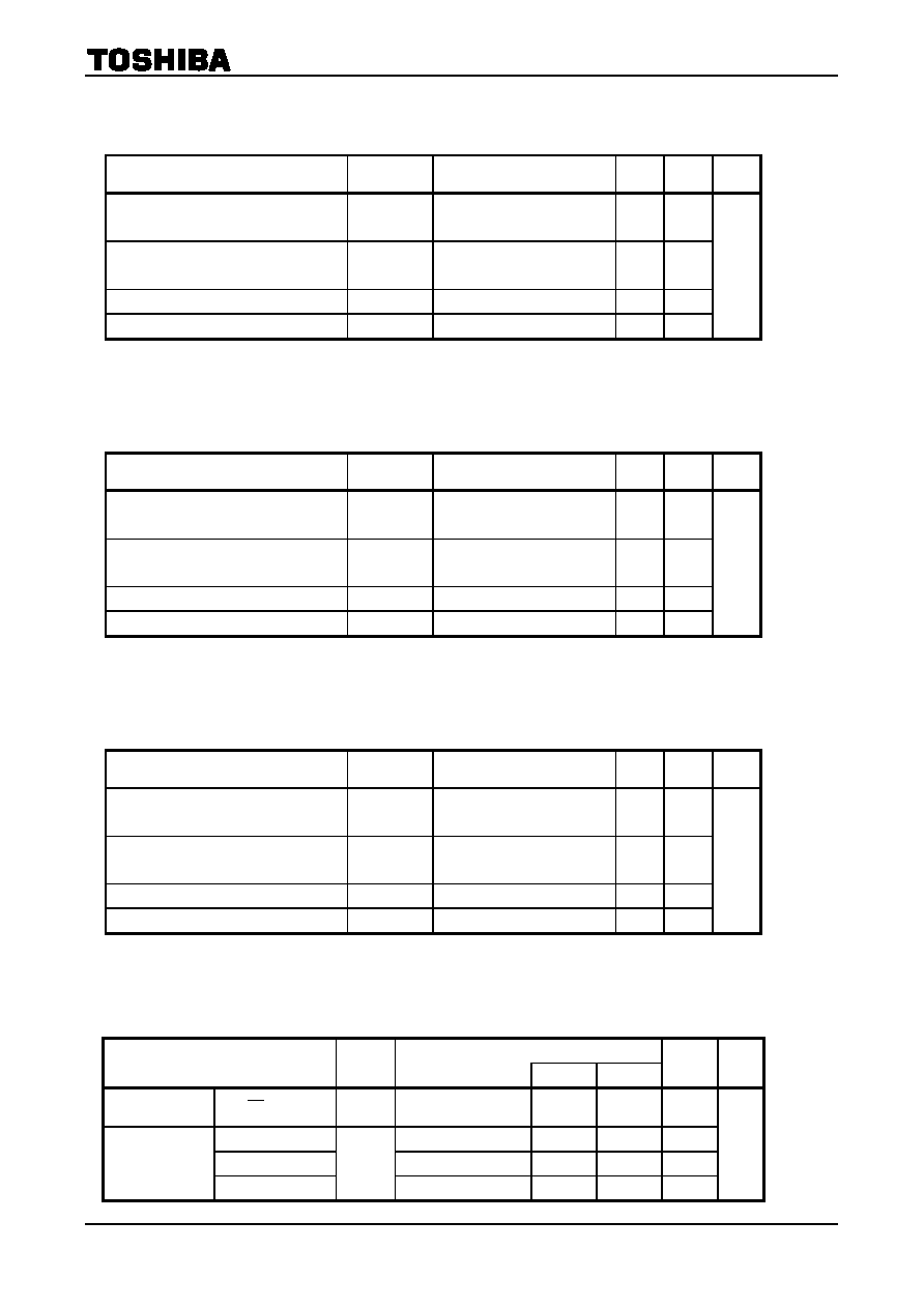
AC Characteristics (Ta
= 40 to 85°C, Input: tr = tf = 2.0 ns,f=10kHz)
VCCA= 3.3 ± 0.3 V, VCCB= 5.0 ± 0.5 V
Characteristics
Symbol
Test Condition
Min
Max
Unit
Propagation delay time
(Bus to Bus)
tpLH
Figures 3 and 5
(Note)
0.3
Propagation delay time
(Bus to Bus)
tpHL
Figures 3 and 5
(Note)
1.2
Output enable time
tpZL
Figures 4 and 6
9.0
Output disable time
tpLZ
Figures 4 and 6
11.0
ns
Note: This parameter is guaranteed by design but is not tested. The bus switch contributes no propagation delay
other than the RC delay of the typical On resistance of the switch and the 30 pF load capacitance, when
driven by an ideal voltage the source (zero output impedance).
VCCA= 2.5 ± 0.2 V, VCCB= 5.0 ± 0.5 V
Characteristics
Symbol
Test Condition
Min
Max
Unit
Propagation delay time
(Bus to Bus)
tpLH
Figures 3 and 5
(Note)
0.35
Propagation delay time
(Bus to Bus)
tpHL
Figures 3 and 5
(Note)
1.8
Output enable time
tpZL
Figures 4 and 6
13.0
Output disable time
tpLZ
Figures 4 and 6
15.0
ns
Note: This parameter is guaranteed by design but is not tested. The bus switch contributes no propagation delay
other than the RC delay of the typical On resistance of the switch and the 30 pF load capacitance, when
driven by an ideal voltage the source (zero output impedance).
VCCA = 2.5 ± 0.2 V, VCCB= 3.3 ± 0.3 V
Characteristics
Symbol
Test Condition
Min
Max
Unit
Propagation delay time
(Bus to Bus)
tpLH
Figures 3 and 5
(Note)
0.45
Propagation delay time
(Bus to Bus)
tpHL
Figures 3 and 5
(Note)
2.2
Output enable time
tpZL
Figures 4 and 6
17.0
Output disable time
tpLZ
Figures 4 and 6
19.0
ns
Note: This parameter is guaranteed by design but is not tested. The bus switch contributes no propagation delay
other than the RC delay of the typical On resistance of the switch and the 30 pF load capacitance, when
driven by an ideal voltage the source (zero output impedance).
Capacitive Characteristics (Ta = 25°C)
Characteristics
Symbol
Test Condition
VCCA (V) VCCB (V)
Typ.
Unit
Control input
capacitance
(OE/ OE , S)
CIN
3.3
3
(1A,2A)
SW=ON (A,B)
3.3
14
(1A,2A)
SW=OFF (A)
3.3
7
Switch
input/output
capacitance
(1B1,1B2,2B1,2B2)
CI/O
SW=OFF (B)
3.3
7
pF
相关PDF资料 |
PDF描述 |
|---|---|
| TC7USB31WBG | DUAL 1-CHANNEL, SGL POLE SGL THROW SWITCH, PBGA8 |
| TC7W53FUTE12L | 2-CHANNEL, SGL ENDED MULTIPLEXER, PDSO8 |
| TC7W53FTE12L | 2-CHANNEL, SGL ENDED MULTIPLEXER, PDSO8 |
| TC7W53F | 2-CHANNEL, SGL ENDED MULTIPLEXER, PDSO8 |
| TC7W53FU | 2-CHANNEL, SGL ENDED MULTIPLEXER, PDSO8 |
相关代理商/技术参数 |
参数描述 |
|---|---|
| TC7MPH3125FK | 功能描述:总线收发器 Bus Transceiver w/Bushold RoHS:否 制造商:Fairchild Semiconductor 逻辑类型:CMOS 逻辑系列:74VCX 每芯片的通道数量:16 输入电平:CMOS 输出电平:CMOS 输出类型:3-State 高电平输出电流:- 24 mA 低电平输出电流:24 mA 传播延迟时间:6.2 ns 电源电压-最大:2.7 V, 3.6 V 电源电压-最小:1.65 V, 2.3 V 最大工作温度:+ 85 C 封装 / 箱体:TSSOP-48 封装:Reel |
| TC7MPH3125FK(EL) | 功能描述:总线收发器 Bus Transceiver RoHS:否 制造商:Fairchild Semiconductor 逻辑类型:CMOS 逻辑系列:74VCX 每芯片的通道数量:16 输入电平:CMOS 输出电平:CMOS 输出类型:3-State 高电平输出电流:- 24 mA 低电平输出电流:24 mA 传播延迟时间:6.2 ns 电源电压-最大:2.7 V, 3.6 V 电源电压-最小:1.65 V, 2.3 V 最大工作温度:+ 85 C 封装 / 箱体:TSSOP-48 封装:Reel |
| TC7MPH3125FTG | 功能描述:总线收发器 INCORRECT MOUSER P/N w/Bushold RoHS:否 制造商:Fairchild Semiconductor 逻辑类型:CMOS 逻辑系列:74VCX 每芯片的通道数量:16 输入电平:CMOS 输出电平:CMOS 输出类型:3-State 高电平输出电流:- 24 mA 低电平输出电流:24 mA 传播延迟时间:6.2 ns 电源电压-最大:2.7 V, 3.6 V 电源电压-最小:1.65 V, 2.3 V 最大工作温度:+ 85 C 封装 / 箱体:TSSOP-48 封装:Reel |
| TC7MPH3125FTG(EB) | 功能描述:总线收发器 Bus Transceiver RoHS:否 制造商:Fairchild Semiconductor 逻辑类型:CMOS 逻辑系列:74VCX 每芯片的通道数量:16 输入电平:CMOS 输出电平:CMOS 输出类型:3-State 高电平输出电流:- 24 mA 低电平输出电流:24 mA 传播延迟时间:6.2 ns 电源电压-最大:2.7 V, 3.6 V 电源电压-最小:1.65 V, 2.3 V 最大工作温度:+ 85 C 封装 / 箱体:TSSOP-48 封装:Reel |
| TC7MPH3245FTG | 功能描述:总线收发器 Bus Trancvr Bushold 8-Bit Bidrectional RoHS:否 制造商:Fairchild Semiconductor 逻辑类型:CMOS 逻辑系列:74VCX 每芯片的通道数量:16 输入电平:CMOS 输出电平:CMOS 输出类型:3-State 高电平输出电流:- 24 mA 低电平输出电流:24 mA 传播延迟时间:6.2 ns 电源电压-最大:2.7 V, 3.6 V 电源电压-最小:1.65 V, 2.3 V 最大工作温度:+ 85 C 封装 / 箱体:TSSOP-48 封装:Reel |
发布紧急采购,3分钟左右您将得到回复。