- 您现在的位置:买卖IC网 > PDF目录98181 > TC820C/LW 1-CH 3-BIT DUAL-SLOPE ADC, PARALLEL ACCESS, PQCC44 PDF资料下载
参数资料
| 型号: | TC820C/LW |
| 元件分类: | ADC |
| 英文描述: | 1-CH 3-BIT DUAL-SLOPE ADC, PARALLEL ACCESS, PQCC44 |
| 封装: | PLASTIC, LCC-44 |
| 文件页数: | 5/34页 |
| 文件大小: | 435K |
| 代理商: | TC820C/LW |
第1页第2页第3页第4页当前第5页第6页第7页第8页第9页第10页第11页第12页第13页第14页第15页第16页第17页第18页第19页第20页第21页第22页第23页第24页第25页第26页第27页第28页第29页第30页第31页第32页第33页第34页
2007 Microchip Technology Inc.
DS21476C-page 13
TC820
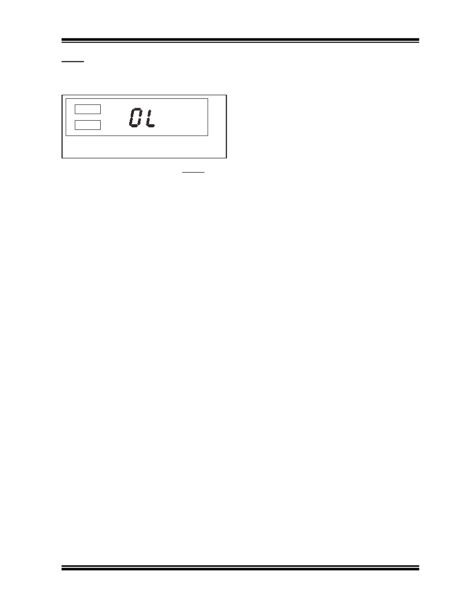
When the logic probe function is selected while FREQ/
VOLTS is low (A/D mode), the ADC will remain in the
Auto-Zero mode. The LCD will read "OL" and all
decimal points will be off (Figure ).
FIGURE 3-6:
LCD Reading.
If the logic probe is active while FREQ/VOLTS is high
(Counter mode), the frequency counter will continue to
operate. The display will read "OL" but the decimal
points will be visible. If the logic probe input is also
connected to the RANGE/FREQ input, bringing the
LOGIC input low will immediately display the frequency
at the logic probe input.
3.5
Analog Pin Functional Description
3.5.1
DIFFERENTIAL SIGNAL INPUTS
(VIN+), (VIN-)
The TC820 is designed with true differential inputs, and
accepts input signals within the Input Stage Common
mode voltage (VCM) range. The typical range is
VDD –1V to VSS + 1.5V. Common mode voltages are
removed from the system when the TC820 operates
from a battery or floating power source (isolated from
measured system) and VSS is connected to analog
common (see Figure 3-5).
In systems where Common mode voltages exist, the
86 dB Common mode rejection ratio minimizes error.
Common mode voltages do, however, affect the
integrator output level. A worst case condition exists if
a large, positive VCM exists in conjunction with a full
scale, negative differential signal. The negative signal
drives the integrator output positive along with VCM
(Figure 3-6). For such applications, the integrator
output swing can be reduced below the recommended
2V full scale swing. The integrator output will swing
within 0.3V of VDD, or VDD without increased linearity
error.
3.5.2
REFERENCE (VDD, VSS)
The TC820 reference, like the analog signal input, has
true differential inputs. In addition, the reference
voltage can be generated anywhere within the power
supply voltage of the converter. The differential
reference inputs permit ratiometric measurements and
simplify interfacing with sensors, such as load cells and
temperature sensors.
To prevent rollover type errors from being induced by
large Common mode voltages, CREF should be large
compared to stray node capacitance. A 0.1 F
capacitor is typical.
The TC820 offers a significantly improved analog
common temperature coefficient, providing a very
stable voltage suitable for use as a voltage reference.
The temperature coefficient of analog common is
typically 35 ppm/°C.
3.5.3
ANALOG COMMON
The analog common pin is set at a voltage potential
approximately 3.3V below VDD. This potential is
between 3.15V and 3.45V below VDD. Analog common
is tied internally to an N-channel FET capable of sink-
ing 3 mA. This FET will hold the common line at 3.3V
below VDD should an external load attempt to pull the
common line toward VDD. Analog common source
current is limited to 12 A, and is, therefore, easily
pulled to a more negative voltage (i.e., below VDD –
3.3V).
The TC820 connects the internal VIN+ and VIN- inputs
to analog common during the auto-zero cycle. During
the reference integrate phase, VIN- is connected to
analog common. If VIN- is not externally connected to
analog common, a Common mode voltage exists.
This is rejected by the converter's 86 dB Common
mode rejection ratio. In battery powered applications,
analog common and VIN- are usually connected,
removing Common mode voltage concerns. In systems
where VIN- is connected to the power supply ground or
to a given voltage, analog common should be
connected to VIN-.
The analog common pin serves to set the analog
section reference or common point. The TC820 is
specifically designed to operate from a battery, or in
any “measurement" system where input signals are not
referenced (float), with respect to the TC820 power
source. The analog common potential of VDD – 3.3V
gives a 7V end of battery life voltage. The analog
common potential has a voltage coefficient of 0.001%.
With
a
sufficiently
high
total
supply
voltage
(VDD –VSS > 7V), analog common is a very stable
potential with excellent temperature stability (typically
35ppm/°C). This potential can be used to generate the
TC820
reference
voltage.
An
external
voltage
reference will be unnecessary in most cases, because
of the 35 ppm/°C temperature coefficient. See the
applications section for details.
High
Low
*
**
* "High" Annuciator will be on when DP1/HI = Logic High
** "Low" Annunciator and Buzzer will be on when DP0/LO = Logic High
相关PDF资料 |
PDF描述 |
|---|---|
| TC820C/PL | 1-CH 3-BIT DUAL-SLOPE ADC, PARALLEL ACCESS, PDIP40 |
| TC820C/KW | 1-CH 3-BIT DUAL-SLOPE ADC, PARALLEL ACCESS, PQFP44 |
| TC820CKWTR | 1-CH DUAL-SLOPE ADC, PQFP44 |
| TC820CLWTR | 1-CH DUAL-SLOPE ADC, PQCC44 |
| TC820CKW | 1-CH DUAL-SLOPE ADC, PQFP44 |
相关代理商/技术参数 |
参数描述 |
|---|---|
| TC820CLW713 | 功能描述:LCD 驱动器 3-3/4 A/D Converter RoHS:否 制造商:Maxim Integrated 数位数量:4.5 片段数量:30 最大时钟频率:19 KHz 工作电源电压:3 V to 3.6 V 最大工作温度:+ 85 C 最小工作温度:- 20 C 封装 / 箱体:PDIP-40 封装:Tube |
| TC820CPL | 功能描述:LCD 驱动器 3-3/4 A/D Converter RoHS:否 制造商:Maxim Integrated 数位数量:4.5 片段数量:30 最大时钟频率:19 KHz 工作电源电压:3 V to 3.6 V 最大工作温度:+ 85 C 最小工作温度:- 20 C 封装 / 箱体:PDIP-40 封装:Tube |
| TC8-20S2405R | 制造商:TRUMPOWER 制造商全称:Tumbler Technologies + TRUMPower 功能描述:DC/DC CONVERTERS 2:1 Input, 12.5 to 20 Watt |
| TC8-20S4805R | 制造商:TRUMPOWER 制造商全称:Tumbler Technologies + TRUMPower 功能描述:DC/DC CONVERTERS 2:1 Input, 12.5 to 20 Watt |
| TC-821-SC | 制造商:Thomas & Betts 功能描述:Cable Accessories Thin Wall Conduit Fitting Zinc Die Cast |
发布紧急采购,3分钟左右您将得到回复。