- 您现在的位置:买卖IC网 > PDF目录98183 > TC850IJL 1-CH 15-BIT MULTI-SLOPE ADC, PARALLEL ACCESS, CDIP40 PDF资料下载
参数资料
| 型号: | TC850IJL |
| 元件分类: | ADC |
| 英文描述: | 1-CH 15-BIT MULTI-SLOPE ADC, PARALLEL ACCESS, CDIP40 |
| 封装: | CERDIP-40 |
| 文件页数: | 4/26页 |
| 文件大小: | 417K |
| 代理商: | TC850IJL |
TC850
DS21479C-page 12
2006 Microchip Technology Inc.
6.0
DIGITAL SECTION
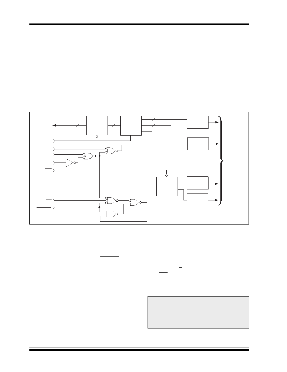
DESCRIPTION
The TC850 digital section consists of two sets of con-
version counters, control and sequencing logic, clock
oscillator and divider, data latches and an 8-bit, 3-state
interface bus. A simplified schematic of the bus
interface logic is shown in Figure 6-1
6.1
Clock Oscillator
The TC850 includes a crystal oscillator on-chip. All that
is required is to connect a crystal across OSC1 and
OSC2 pins and to add two inexpensive capacitors
(Figure 1-1). The oscillator output is ÷ 4 prior to clock-
ing the A/D internal counters. For example, a 100 kHz
crystal produces a system clock frequency of 25 kHz.
Since each conversion requires 1280 clock periods, in
this case the conversion rate will be 25,000/1280, or
19.5 conversions per second.
In most applications, however, an external clock is
divided down from the microprocessor clock. In this
case, the OSC1 pin is used as the external oscillator
input and OSC2 is left unconnected. The external clock
driver should swing from digital ground to VDD. The ÷ 4
function is active for both external clock and crystal
oscillator operations.
FIGURE 6-1:
Bus Interface Simplified Schematic
6.2
Digital Operating Modes
Two modes of operation are available with the TC850,
continuous conversions and on-demand. The Operat-
ing mode is controlled by the CONT/DEMAND input.
The bus interface method is different for Continuous
and Demand modes of operation.
6.2.1
DEMAND MODE OPERATION
When CONT/DEMAND is low, the TC850 performs one
conversion each time the chip is selected and the WR
input is pulsed low. Data is valid on the falling edge of
the BUSY output and can be accessed using the
interface truth table (Table 6-1).
6.2.2
CONTINUOUS MODE OPERATION
When CONT/DEMAND is high, the TC850 continu-
ously performs conversions. Data will be valid on the
falling edge of the BUSY output and remains valid for
443-1/2 clock cycles.
The low/high (L/H) byte-select and overrange/polarity
(OVR/POL) inputs are disabled during Continuous mode
operation. Data must be read in three consecutive bytes,
as shown in Table 6-1.
RD
L/H
3-State
Buffer
Output
Enable
End of Conversion
CONT/
DEMAND
Start
Conversion
To A/D
Control Logic
Octal
2-Input Mux
Select
Low-Byte
Up/Down
Counter
High-Byte
Up/Down
Counter
Polarity
Overrange
TC850
8
Select
2-Input Mux
DBO–DB7
8
7
8
CE
CS
WR
POL/OVR
Note:
In Continuous mode, the conversion result
must be read within 443-1/2 clock cycles
of the BUSY output falling edge. After this
time (i.e.,1/2 clock cycle before BUSY
goes high) the internal counters are reset
and the data is lost.
相关PDF资料 |
PDF描述 |
|---|---|
| TC850ILW713 | 1-CH 15-BIT MULTI-SLOPE ADC, PARALLEL ACCESS, PQCC44 |
| TC850ILWTR | 1-CH 15-BIT MULTI-SLOPE ADC, PARALLEL ACCESS, PQCC44 |
| TC850CLW | 1-CH 15-BIT MULTI-SLOPE ADC, PARALLEL ACCESS, PQCC44 |
| TC850CLWTR | 1-CH 15-BIT MULTI-SLOPE ADC, PARALLEL ACCESS, PQCC44 |
| TC850CLW713 | 1-CH 15-BIT MULTI-SLOPE ADC, PARALLEL ACCESS, PQCC44 |
相关代理商/技术参数 |
参数描述 |
|---|---|
| TC850ILW | 功能描述:模数转换器 - ADC 16 Bit Hi Speed A/D RoHS:否 制造商:Texas Instruments 通道数量:2 结构:Sigma-Delta 转换速率:125 SPs to 8 KSPs 分辨率:24 bit 输入类型:Differential 信噪比:107 dB 接口类型:SPI 工作电源电压:1.7 V to 3.6 V, 2.7 V to 5.25 V 最大工作温度:+ 85 C 安装风格:SMD/SMT 封装 / 箱体:VQFN-32 |
| TC850ILW713 | 功能描述:模数转换器 - ADC 16 Bit Hi Speed A/D RoHS:否 制造商:Texas Instruments 通道数量:2 结构:Sigma-Delta 转换速率:125 SPs to 8 KSPs 分辨率:24 bit 输入类型:Differential 信噪比:107 dB 接口类型:SPI 工作电源电压:1.7 V to 3.6 V, 2.7 V to 5.25 V 最大工作温度:+ 85 C 安装风格:SMD/SMT 封装 / 箱体:VQFN-32 |
| TC8521AM | 制造商:TOSHIBA 制造商全称:Toshiba Semiconductor 功能描述:REAL TIME CLOCK ケ |
| TC8521AP | 制造商:TOSHIBA 制造商全称:Toshiba Semiconductor 功能描述:REAL TIME CLOCK ケ |
| TC8566AF | 制造商:TOSHIBA 制造商全称:Toshiba Semiconductor 功能描述:FLOPPY DISK CONTROLLER |
发布紧急采购,3分钟左右您将得到回复。