- 您现在的位置:买卖IC网 > PDF目录85438 > TCM810LVNB713 1-CHANNEL POWER SUPPLY SUPPORT CKT, PDSO3 PDF资料下载
参数资料
| 型号: | TCM810LVNB713 |
| 元件分类: | 电源管理 |
| 英文描述: | 1-CHANNEL POWER SUPPLY SUPPORT CKT, PDSO3 |
| 封装: | SOT-23B, 3 PIN |
| 文件页数: | 2/6页 |
| 文件大小: | 41K |
| 代理商: | TCM810LVNB713 |
2
TCM809/810-4 11/30/99
TCM809
TCM810
3-Pin Microprocessor Reset Monitors
ABSOLUTE MAXIMUM RATINGS*
Supply Voltage (VCC to GND) ................................ +6.0V
RESET, RESET ............................ – 0.3V to (VCC + 0.3V)
Input Current, VCC.. .................................................. 20mA
Output Current, RESET, RESET ............................. 20mA
dV/dt (VCC) ....................................................... 100V/sec
Operating Temperature Range ............. – 40
°C to +125°C
Power Dissipation (TA ≤ 70°C)
3-Pin SOT-23B (derate 4mW/
°C above +70°C) 230mW
Storage Temperature Range ................ – 65
°C to +150°C
Lead Temperature (Soldering, 10 sec) ................. +260
°C
*This is a stress rating only and functional operation of the device at these
or any other conditions above those indicated in the operational sections of
the specifications is not implied. Exposure to Absolute Maximum Rating
Conditions for extended periods may affect device reliability.
PIN DESCRIPTION
Pin No.
(3-Pin SOT-23B)
Symbol
Description
1
GND
Ground
2
RESET (TCM809)
RESET output remains low while VCC is below the reset voltage threshold, and
for 240msec (140msec min.) after VCC rises above reset threshold.
2
RESET (TCM810)
RESET output remains high while VCC is below the reset voltage threshold,
and for 240msec (140msec min.) after VCC rises above reset threshold.
3VCC
Supply voltage (Typ. +3.0V to +5.0V)
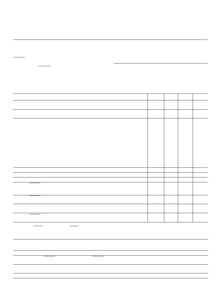
Symbol Parameter
Test Conditions
Min
Typ
Max
Unit
VCC Range
TA = 0°C to +70°C
1.0
—
5.5
V
TA = – 40°C to +125°C
1.2
—
5.5
ICC
Supply Current
TCM8xxL/M/J VCC < 5.5V
—
24
60
A
TCM8xxR/S/T: VCC < 3.6V
—
17
50
VTH
Reset Threshold (Note 2)
TCM8xxL: TA = +25°C
4.56
4.63
4.70
V
TA = – 40°C to +125°C
4.50
—
4.75
TCM8xxM: TA = +25°C
4.31
4.38
4.45
TA = – 40°C to +125°C
4.25
—
4.50
TCM809J: TA = +25°C
3.93
4.00
4.06
TA = – 40°C to +125°C
3.89
—
4.10
TCM8xxT: TA = +25°C
3.04
3.08
3.11
TA = – 40°C to +125°C
3.00
—
3.15
TCM8xxS: TA = +25°C
2.89
2.93
2.96
TA = – 40°C to +125°C
2.85
—
3.00
TCM8xxR: TA = +25°C
2.59
2.63
2.66
TA = – 40°C to +125°C
2.55
—
2.70
Reset Threshold Tempco
—
30
—
ppm/
°C
VCC to Reset Delay (Note 2)
VCC = VTH to (VTH – 100mV)
—
20
—
sec
Reset Active Timeout Period
140
240
560
msec
VOL
RESET Output Voltage Low
TCM809R/S/T: VCC = VTH min, ISINK = 1.2mA
——
0.3
V
(TCM809)
TCM809L/M/J: VCC = VTH min, ISINK = 3.2mA
——
0.4
VCC > 1.0V, ISINK = 50A
——
0.3
VOH
RESET Output Voltage High
TCM809R/S/T: VCC > VTH max, ISOURCE = 500A
0.8 VCC
——
V
(TCM809)
TCM809L/M/J: VCC > VTH max, ISOURCE = 800AVCC – 1.5
——
VOL
RESET Output Voltage Low
TCM810R/S/T: VCC = VTH max, ISINK = 1.2mA
——
0.3
V
(TCM810)
TCM810L/M/J: VCC = VTH max, ISINK = 3.2mA
——
0.4
VOH
RESET Output Voltage High
1.8 < VCC < VTH min, ISOURCE = 150A
0.8 VCC
——
V
(TCM810)
NOTES:
1. Production testing done at TA = +25°C, over temperature limits guaranteed by design.
2. RESET output for TCM809, RESET Output for TCM810.
ELECTRICAL CHARACTERISTICS:
Vcc = Full Range, TA = Operating Temperature Range unless other-
wise noted. Typical values are at TA = +25°C, VCC = 5V for L/M/J, 3.3V forT/S, 3.0V for R (Note 1).
相关PDF资料 |
PDF描述 |
|---|---|
| TCM810RVNBTR | 1-CHANNEL POWER SUPPLY SUPPORT CKT, PDSO3 |
| TC54VC1501MBTR | 1-CHANNEL POWER SUPPLY SUPPORT CKT, PSSO3 |
| TC54VN1501MBRT | 1-CHANNEL POWER SUPPLY SUPPORT CKT, PSSO3 |
| TC54VN2501ECB723 | 1-CHANNEL POWER SUPPLY SUPPORT CKT, PDSO3 |
| TC54VC3802EMB713 | 1-CHANNEL POWER SUPPLY SUPPORT CKT, PSSO3 |
相关代理商/技术参数 |
参数描述 |
|---|---|
| TCM810MEB713 | 制造商:MICROCHIP 制造商全称:Microchip Technology 功能描述:3-Pin Microcontroller Reset Monitors |
| TCM810MELB713 | 制造商:MICROCHIP 制造商全称:Microchip Technology 功能描述:3-Pin Microcontroller Reset Monitors |
| TCM810MEN | 制造商:MICROCHIP 制造商全称:Microchip Technology 功能描述:3-Pin Microcontroller Reset Monitors |
| TCM810MENB | 制造商:TELCOM 制造商全称:TelCom Semiconductor, Inc 功能描述:3-PIN UP RESET MONITORS |
| TCM810MENB713 | 功能描述:监控电路 Microprocessor 4.38V RoHS:否 制造商:STMicroelectronics 监测电压数: 监测电压: 欠电压阈值: 过电压阈值: 输出类型:Active Low, Open Drain 人工复位:Resettable 监视器:No Watchdog 电池备用开关:No Backup 上电复位延迟(典型值):10 s 电源电压-最大:5.5 V 最大工作温度:+ 85 C 安装风格:SMD/SMT 封装 / 箱体:UDFN-6 封装:Reel |
发布紧急采购,3分钟左右您将得到回复。