- 您现在的位置:买卖IC网 > PDF目录85416 > TDA8752AH/6/C4 (NXP SEMICONDUCTORS) 3-CH 8-BIT PROPRIETARY METHOD ADC, PARALLEL ACCESS, PQFP100 PDF资料下载
参数资料
| 型号: | TDA8752AH/6/C4 |
| 厂商: | NXP SEMICONDUCTORS |
| 元件分类: | ADC |
| 英文描述: | 3-CH 8-BIT PROPRIETARY METHOD ADC, PARALLEL ACCESS, PQFP100 |
| 封装: | PLASTIC, SOT-317-2, QFP-64 |
| 文件页数: | 10/40页 |
| 文件大小: | 250K |
| 代理商: | TDA8752AH/6/C4 |
第1页第2页第3页第4页第5页第6页第7页第8页第9页当前第10页第11页第12页第13页第14页第15页第16页第17页第18页第19页第20页第21页第22页第23页第24页第25页第26页第27页第28页第29页第30页第31页第32页第33页第34页第35页第36页第37页第38页第39页第40页
1999 Feb 24
18
Philips Semiconductors
Product specication
Triple high-speed Analog-to-Digital
Converter (ADC)
TDA8752A
OFFSET REGISTER
This register controls the clamp level for the
RGB channels. The relationship between the
programming code and the level of the clamp code is given
in Table 2.
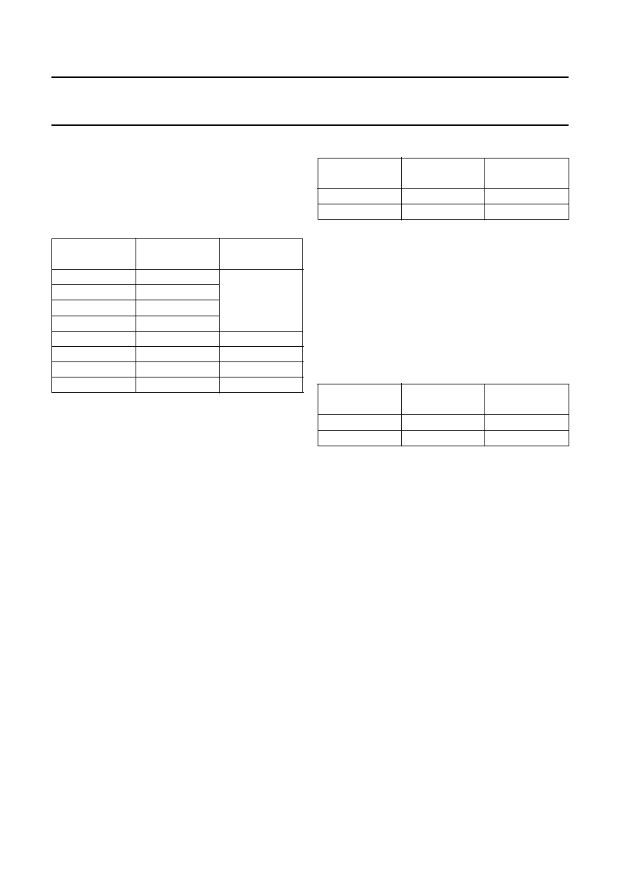
Table 2
Coding
The default programmed value is:
Programmed code = 127
Clamp code = 0
ADC output = 0.
COARSE AND FINE REGISTERS
These two registers enable the gain control, the AGC gain
with the coarse register and the reference voltage with the
fine register. The coarse register programming equation is
as follows:
Where: Vref = 2.5 V.
The gain correspondence is given in Table 3. The gain is
linear with reference to the programming code (NFINE = 0).
PROGRAMMED
CODE
CLAMP CODE
ADC OUTPUT
0
63.5
underow
1
63
2
62.5
↓↓
127
0
↓↓↓
254
63.5
63 or 64
255
64
GAIN
N
COARSE
1
+
V
ref 1
N
FINE
32
16
×
-------------------
–
----------------------------------------------
1
16
------
×
N
COARSE
1
+
V
ref 512
N
FINE
–
()
-------------------------------------------------
32
×
=
Table 3
Gain correspondence (COARSE)
The default programmed value is as follows:
N
COARSE =32
Gain = 0.825
Vi to be full-scale = 1.212.
To modulate this gain, the fine register is programmed
using the above equation. With a full-scale ADC input, the
fine register resolution is a 1
2LSB peak-to-peak
(see Table 4 for NCOARSE = 32).
Table 4
Gain correspondence (FINE)
The default programmed value is: NFINE =0.
CONTROL REGISTER
COAST and HSYNC signals can be inverted by setting the
I2C-bus control bits V level and H level respectively. When
V level and H level are set to zero respectively, COAST
and HSYNC are active HIGH.
The bit ‘edge’ defines the rising or falling edge of CKREF
to synchronise the PLL. It will be on the rising edge if the
bit is at logic 0 and on the falling edge if the bit is at logic 1.
The bits Up and Do are used for the test, to force the
charge pump current. These bits have to be logic 0 during
normal use.
The bits Ip0, Ip1 and Ip2 control the charge pump current,
to increase the bandwidth of the PLL, as shown in Table 5.
NCOARSE
GAIN
Vi TO BE
FULL-SCALE
32
0.825
1.212
99
2.5
0.4
NFINE
GAIN
Vi TO BE
FULL-SCALE
0
0.825
1.212
31
0.878
1.139
相关PDF资料 |
PDF描述 |
|---|---|
| TDA8752AH/8/C4/S1 | 3-CH 8-BIT PROPRIETARY METHOD ADC, PARALLEL ACCESS, PQFP100 |
| TDA8752AH8BA-S | 3-CH 8-BIT PROPRIETARY METHOD ADC, PARALLEL ACCESS, PQFP100 |
| TDA8752AH8BA | 3-CH 8-BIT PROPRIETARY METHOD ADC, PARALLEL ACCESS, PQFP100 |
| TDA8775GB-T | TRIPLE, PARALLEL, WORD INPUT LOADING, 0.01 us SETTLING TIME, 10-BIT DAC, PQFP48 |
| TDA8706AMDB | 3-CH 6-BIT PROPRIETARY METHOD ADC, PARALLEL ACCESS, PDSO24 |
相关代理商/技术参数 |
参数描述 |
|---|---|
| TDA8752AH8BA | 制造商: 功能描述: 制造商:undefined 功能描述: |
| TDA8752B | 制造商:PHILIPS 制造商全称:NXP Semiconductors 功能描述:Triple high-speed Analog-to-Digital Converter 110 Msps ADC |
| TDA8752BH | 制造商:PHILIPS 制造商全称:NXP Semiconductors 功能描述:Triple high-speed Analog-to-Digital Converter 110 Msps ADC |
| TDA8752BH/8 | 制造商:PHILIPS 制造商全称:NXP Semiconductors 功能描述:Triple high-speed Analog-to-Digital Converter 110 Msps ADC |
| TDA8752H | 制造商:PHILIPS 制造商全称:NXP Semiconductors 功能描述:Triple high speed Analog-to-Digital Converter ADC |
发布紧急采购,3分钟左右您将得到回复。