- 您现在的位置:买卖IC网 > PDF目录85416 > TDA8752AH8BA-S (NXP SEMICONDUCTORS) 3-CH 8-BIT PROPRIETARY METHOD ADC, PARALLEL ACCESS, PQFP100 PDF资料下载
参数资料
| 型号: | TDA8752AH8BA-S |
| 厂商: | NXP SEMICONDUCTORS |
| 元件分类: | ADC |
| 英文描述: | 3-CH 8-BIT PROPRIETARY METHOD ADC, PARALLEL ACCESS, PQFP100 |
| 封装: | PLASTIC, SOT-317-2, QFP-64 |
| 文件页数: | 11/40页 |
| 文件大小: | 250K |
| 代理商: | TDA8752AH8BA-S |
第1页第2页第3页第4页第5页第6页第7页第8页第9页第10页当前第11页第12页第13页第14页第15页第16页第17页第18页第19页第20页第21页第22页第23页第24页第25页第26页第27页第28页第29页第30页第31页第32页第33页第34页第35页第36页第37页第38页第39页第40页
1999 Feb 24
19
Philips Semiconductors
Product specication
Triple high-speed Analog-to-Digital
Converter (ADC)
TDA8752A
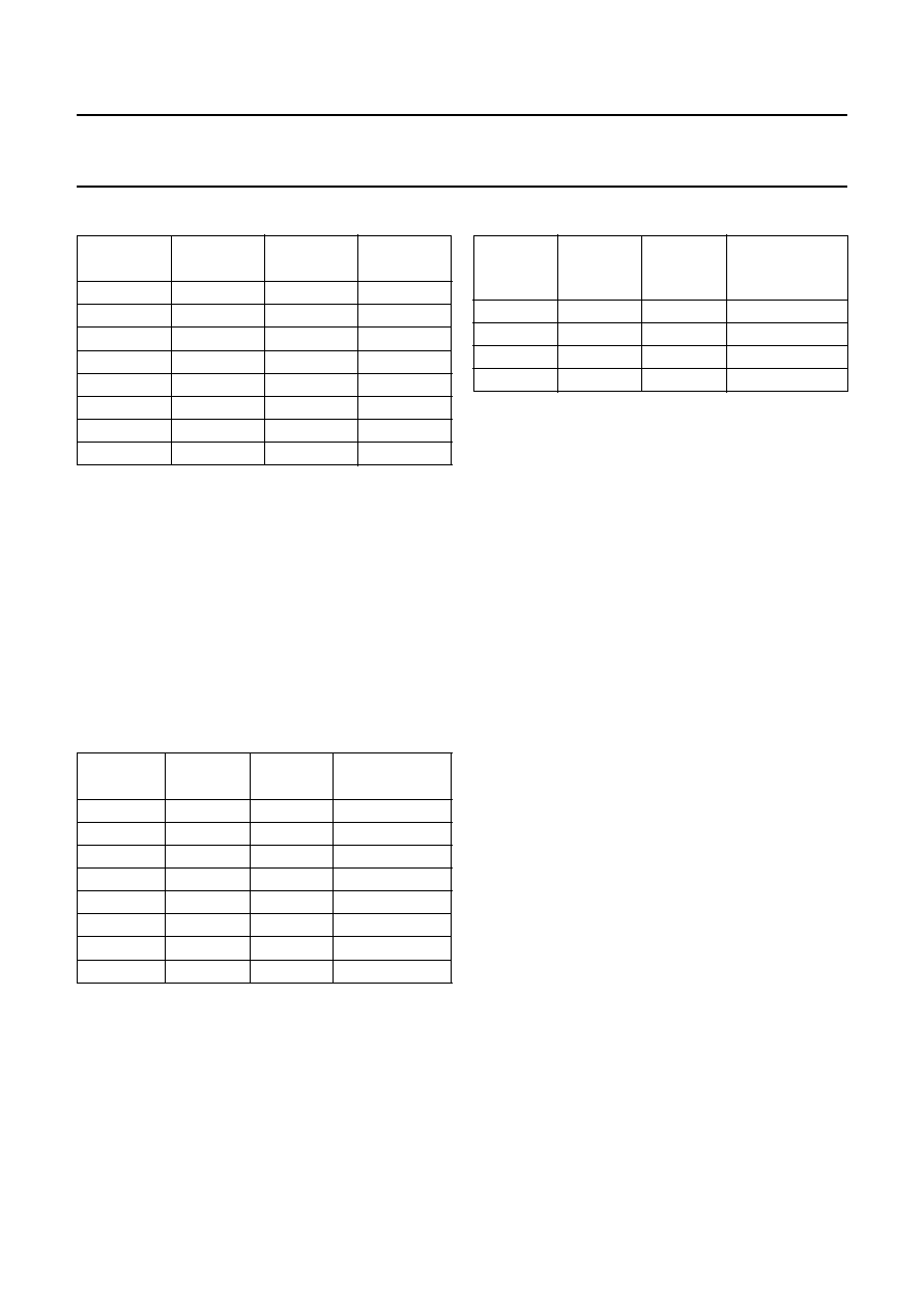
Table 5
Charge-pump current control
The default programmed value is as follows:
Charge pump current = 100 A
Test bits: no test mode; bits Up and Do at logic 0
Rising edge of CKREF: bit edge at logic 0
COAST and HSYNC inputs are active HIGH: V level and
H level at logic 0.
VCO REGISTER
The bits Z2, Z1 and Z0 enable the internal resistance for
the VCO filter to be selected.
Table 6
VCO register bits
Ip2
Ip1
Ip0
CURRENT
(
A)
0
6.25
0
1
12.5
010
25
011
50
100
101
200
110
400
111
700
Z2
Z1
Z0
RESISTANCE
(k
)
0
high impedance
0
1
128
01
0
32
01
1
16
10
0
8
10
1
4
11
0
2
11
1
Table 7
VCO gain control
The bits VCO1 and VCO0 control the VCO gain.
The default programmed value is as follows:
Internal resistance = 16 k
VCO gain = 15 MHz/V.
DIVIDER REGISTER
This register controls the PLL frequency. The bits are the
LSB bits.
The default programmed value is 0011 0010 0000 = 800.
The MSB bits (Di11, Di10 and Di9) and the LSB bit (Di0)
have to be programmed before the bits Di8 to Di1 to have
the required divider ratio. The bit Di0 is used for the parity
divider number = Di0 = 0 = even number Di0 = 1 = odd
number. It should be noted that if the I2C-bus programming
is done in mode = 1 and the bit Di0 has to be toggled, then
the registers have to be loaded twice to have the update
divider ratio.
POWER-DOWN MODE
When the supply is completely switched off, the
registers are set to their default values; in that event they
have to be reprogrammed if the required settings are
different (e.g. through an EEPROM)
When the device is in power-down mode, the previously
programmed register values remain unaffected.
PHASEA AND PHASEB REGISTERS
The bit Cka is logic 0 when the used clock is the PLL clock,
and logic 1 when the used clock is the external clock.
The bit Ckb is logic 0 when the second clock is not used.
The bits Pa4 to Pa0 and Pb4 to Pb0 are used to program
the phase shift for the clock, CKADCO, CKAO and CKBO
(see Table 8).
VCO1
VCO0
VCO gain
(MHz/V)
PIXEL CLOCK
FREQUENCY
RANGE (MHz)
1
0
60
10 to 17
0
1
30
17 to 35
1
0
60
35 to 60
1
100
60 to 100
相关PDF资料 |
PDF描述 |
|---|---|
| TDA8752AH8BA | 3-CH 8-BIT PROPRIETARY METHOD ADC, PARALLEL ACCESS, PQFP100 |
| TDA8775GB-T | TRIPLE, PARALLEL, WORD INPUT LOADING, 0.01 us SETTLING TIME, 10-BIT DAC, PQFP48 |
| TDA8706AMDB | 3-CH 6-BIT PROPRIETARY METHOD ADC, PARALLEL ACCESS, PDSO24 |
| TDA8764AHL/6/C1 | 1-CH 10-BIT PROPRIETARY METHOD ADC, PARALLEL ACCESS, PQFP32 |
| TDA8764ATS/6/C1 | 1-CH 10-BIT PROPRIETARY METHOD ADC, PARALLEL ACCESS, PDSO28 |
相关代理商/技术参数 |
参数描述 |
|---|---|
| TDA8752B | 制造商:PHILIPS 制造商全称:NXP Semiconductors 功能描述:Triple high-speed Analog-to-Digital Converter 110 Msps ADC |
| TDA8752BH | 制造商:PHILIPS 制造商全称:NXP Semiconductors 功能描述:Triple high-speed Analog-to-Digital Converter 110 Msps ADC |
| TDA8752BH/8 | 制造商:PHILIPS 制造商全称:NXP Semiconductors 功能描述:Triple high-speed Analog-to-Digital Converter 110 Msps ADC |
| TDA8752H | 制造商:PHILIPS 制造商全称:NXP Semiconductors 功能描述:Triple high speed Analog-to-Digital Converter ADC |
| TDA8752H/6 | 制造商:PHILIPS 制造商全称:NXP Semiconductors 功能描述:Triple high speed Analog-to-Digital Converter ADC |
发布紧急采购,3分钟左右您将得到回复。