- 您现在的位置:买卖IC网 > PDF目录98217 > THS1030CDWR (TEXAS INSTRUMENTS INC) 1-CH 10-BIT PROPRIETARY METHOD ADC, PARALLEL ACCESS, PDSO28 PDF资料下载
参数资料
| 型号: | THS1030CDWR |
| 厂商: | TEXAS INSTRUMENTS INC |
| 元件分类: | ADC |
| 英文描述: | 1-CH 10-BIT PROPRIETARY METHOD ADC, PARALLEL ACCESS, PDSO28 |
| 封装: | GREEN, PLASTIC, SOIC-28 |
| 文件页数: | 18/37页 |
| 文件大小: | 727K |
| 代理商: | THS1030CDWR |
第1页第2页第3页第4页第5页第6页第7页第8页第9页第10页第11页第12页第13页第14页第15页第16页第17页当前第18页第19页第20页第21页第22页第23页第24页第25页第26页第27页第28页第29页第30页第31页第32页第33页第34页第35页第36页第37页
THS1030
3V TO 5.5V, 10BIT, 30 MSPS
CMOS ANALOGTODIGITAL CONVERTER
SLAS243E NOVEMBER 1999 REVISED DECEMBER 2003
25
POST OFFICE BOX 655303
DALLAS, TEXAS 75265
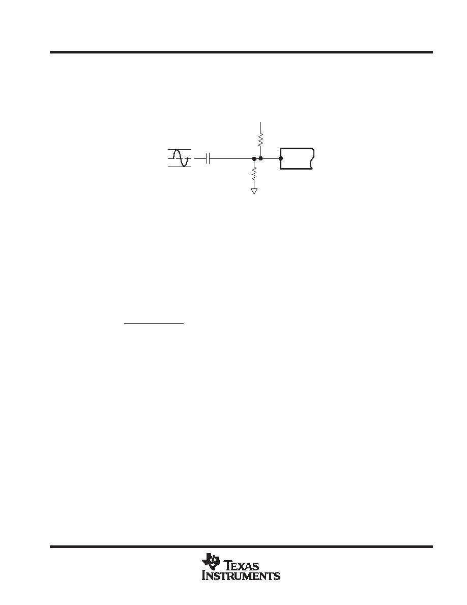
PRINCIPLES OF OPERATION
equivalent input resistance at AIN and ac-coupling to AIN
Some applications may require ac-coupling of the input signal to the AIN pin. Such applications can use an
ac-coupling network such as shown in Figure 29.
AIN
AVDD
R(Bias1)
R(Bias2)
Cin
Figure 29. AC-Coupling the Input Signal to the AIN Pin
Note that if the bias voltage is derived from the supplies, as shown in Figure 29, then additional filtering should
be used to ensure that noise from the supplies does not reach AIN.
Working with the input current pulse equations given in the previous section is awkward when designing
ac-coupling input networks. For such design, it is much simpler to model the AIN input as an equivalent
resistance, RAIN, from the AIN pin to a voltage source VM where
VM = (REFTS + REFBS)/2 and RAIN = 1 / (CS x fclk)
where fclk is the CLK frequency.
The high-pass 3 dB cutoff frequency for the circuit shown in Figure 29 is:
f
(
*3dB) +
1
2
p
R
IN
tot
where RINtot is the parallel combination of Rbias1, Rbias2, and RAIN. This approximation is good provided that
the clock frequency, fclk, is much higher than f(3 dB).
Note also that the effect of the equivalent RAIN and VM at the AIN pin must be allowed for when designing the
bias network dc level.
details
The above value for RAIN is derived by noting that the average AIN voltage must equal the bias voltage supplied
by the ac coupling network. The average value of VLAST in equation 8 is thus a constant voltage
VLAST = V(AIN bias) – VM
For an input voltage Vin at the AIN pin,
Qin = (Vin – VLAST) x Cs
Provided that f (3 dB) is much lower than fclk, a constant current flowing over the clock period can approximate
the input charging pulse
Iin
= Qin / tclk
= Qin x fclk
= (Vin – VLAST) x CS x fclk
(10)
相关PDF资料 |
PDF描述 |
|---|---|
| THS1030CPWRG4 | 1-CH 10-BIT PROPRIETARY METHOD ADC, PARALLEL ACCESS, PDSO28 |
| THS1030IPWR | 1-CH 10-BIT PROPRIETARY METHOD ADC, PARALLEL ACCESS, PDSO28 |
| THS1030CDWG4 | 1-CH 10-BIT PROPRIETARY METHOD ADC, PARALLEL ACCESS, PDSO28 |
| THS1030IDW | 1-CH 10-BIT PROPRIETARY METHOD ADC, PARALLEL ACCESS, PDSO28 |
| THS1030CPWR | 1-CH 10-BIT PROPRIETARY METHOD ADC, PARALLEL ACCESS, PDSO28 |
相关代理商/技术参数 |
参数描述 |
|---|---|
| THS1030CDWRG4 | 功能描述:模数转换器 - ADC 10-Bit 30 MSPS 1-Ch Pin Comp RoHS:否 制造商:Texas Instruments 通道数量:2 结构:Sigma-Delta 转换速率:125 SPs to 8 KSPs 分辨率:24 bit 输入类型:Differential 信噪比:107 dB 接口类型:SPI 工作电源电压:1.7 V to 3.6 V, 2.7 V to 5.25 V 最大工作温度:+ 85 C 安装风格:SMD/SMT 封装 / 箱体:VQFN-32 |
| THS1030CPW | 功能描述:模数转换器 - ADC 10-Bit 30 MSPS 1-Ch Pin Comp RoHS:否 制造商:Texas Instruments 通道数量:2 结构:Sigma-Delta 转换速率:125 SPs to 8 KSPs 分辨率:24 bit 输入类型:Differential 信噪比:107 dB 接口类型:SPI 工作电源电压:1.7 V to 3.6 V, 2.7 V to 5.25 V 最大工作温度:+ 85 C 安装风格:SMD/SMT 封装 / 箱体:VQFN-32 |
| THS1030CPWG4 | 功能描述:模数转换器 - ADC 10-Bit 30 MSPS 1-Ch Pin Comp RoHS:否 制造商:Texas Instruments 通道数量:2 结构:Sigma-Delta 转换速率:125 SPs to 8 KSPs 分辨率:24 bit 输入类型:Differential 信噪比:107 dB 接口类型:SPI 工作电源电压:1.7 V to 3.6 V, 2.7 V to 5.25 V 最大工作温度:+ 85 C 安装风格:SMD/SMT 封装 / 箱体:VQFN-32 |
| THS1030CPWR | 功能描述:模数转换器 - ADC 10-Bit 30 MSPS 1-Ch Pin Comp RoHS:否 制造商:Texas Instruments 通道数量:2 结构:Sigma-Delta 转换速率:125 SPs to 8 KSPs 分辨率:24 bit 输入类型:Differential 信噪比:107 dB 接口类型:SPI 工作电源电压:1.7 V to 3.6 V, 2.7 V to 5.25 V 最大工作温度:+ 85 C 安装风格:SMD/SMT 封装 / 箱体:VQFN-32 |
| THS1030CPWRG4 | 功能描述:模数转换器 - ADC 10-Bit 30 MSPS 1-Ch Pin Comp RoHS:否 制造商:Texas Instruments 通道数量:2 结构:Sigma-Delta 转换速率:125 SPs to 8 KSPs 分辨率:24 bit 输入类型:Differential 信噪比:107 dB 接口类型:SPI 工作电源电压:1.7 V to 3.6 V, 2.7 V to 5.25 V 最大工作温度:+ 85 C 安装风格:SMD/SMT 封装 / 箱体:VQFN-32 |
发布紧急采购,3分钟左右您将得到回复。