- 您现在的位置:买卖IC网 > PDF目录98223 > THS3122CDDA (TEXAS INSTRUMENTS INC) 1 CHANNEL, VIDEO AMPLIFIER, PDSO8 PDF资料下载
参数资料
| 型号: | THS3122CDDA |
| 厂商: | TEXAS INSTRUMENTS INC |
| 元件分类: | 音频/视频放大 |
| 英文描述: | 1 CHANNEL, VIDEO AMPLIFIER, PDSO8 |
| 封装: | GREEN, PLASTIC, SOP-8 |
| 文件页数: | 9/34页 |
| 文件大小: | 1276K |
| 代理商: | THS3122CDDA |
第1页第2页第3页第4页第5页第6页第7页第8页当前第9页第10页第11页第12页第13页第14页第15页第16页第17页第18页第19页第20页第21页第22页第23页第24页第25页第26页第27页第28页第29页第30页第31页第32页第33页第34页
0.205
(5,21)
0.060
(1,52)
0.013
(0,33)
0.017
(0,432)
0.025
(0,64)
0.094
(2,39)
0.040
(1,01)
0.035
(0,89)
0.075
(1,91)
0.010
vias
(0,254)
0.030
(0,76)
Pin1
TopView
P
=
DMax
T
-
max
A
q
JA
SLOS382D
– SEPTEMBER 2001 – REVISED FEBRUARY 2011
PowerPAD
Layout Considerations
transfer.
Therefore,
the
holes
under
the
THS3125/THS3122 PowerPAD package should
make the connection to the internal ground plane
with a complete connection around the entire
circumference of the plated-through hole.
6. The top-side solder mask should leave the
terminals of the package and the thermal pad
area with its five holes exposed. The bottom-side
solder mask should cover the five holes of the
thermal pad area. This configuration prevents
solder from being pulled away from the thermal
pad area during the reflow process.
7. Apply solder paste to the exposed thermal pad
area and all of the IC terminals.
8. With these preparatory steps in place, the IC is
simply placed in position and run through the
solder
reflow
operation
as
any
standard
surface-mount component. This procedure results
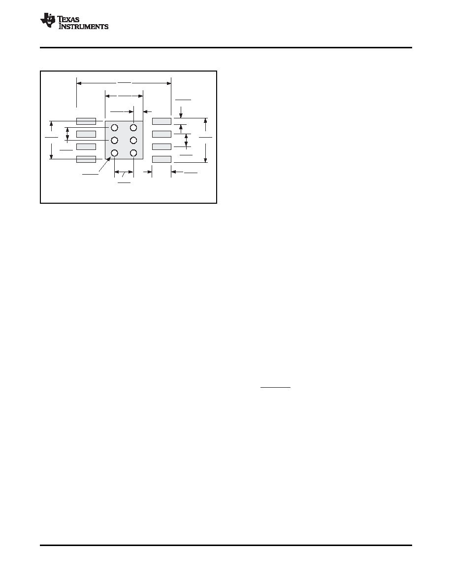
Dimensions are in inches (millimeters).
in a part that is properly installed.
Figure 49. DGN PowerPAD PCB Etch and Via
Power Dissipation and Thermal
Pattern
Considerations
Although there are many ways to properly heatsink
The THS3125 and THS3122 incorporate automatic
the PowerPAD package, the following steps illustrate
thermal shutoff protection. This protection circuitry
the recommended approach.
shuts down the amplifier if the junction temperature
exceeds approximately +160
°C. When the junction
1. PCB with a top side etch pattern as shown in
temperature reduces to approximately +140
°C, the
amplifier turns on again. However, for maximum
2. Place five holes in the area of the thermal pad.
performance and reliability, the designer must take
These holes should be 0.01 inch (0,254 mm) in
care to ensure that the design does not exceed a
diameter. Keep them small so that solder wicking
junction temperature of +125
°C. Between +125°C
through the holes is not a problem during reflow.
and +150
°C, damage does not occur, but the
3. Additional vias may be placed anywhere along
performance of the amplifier begins to degrade and
the thermal plane outside of the thermal pad
long-term
reliability
suffers.
The
thermal
area.
These
vias
help
dissipate
the
heat
characteristics of the device are dictated by the
generated by the THS3125/THS3122 IC. These
package and the PCB. Maximum power dissipation
additional vias may be larger than the 0.01-inch
for a given package can be calculated using the
(0,254-mm) diameter vias directly under the
following formula.
thermal pad. They can be larger because they
are not in the thermal pad area to be soldered so
that wicking is not a problem.
4. Connect all holes to the internal ground plane.
where:
Note that the PowerPAD is electrically isolated
PDMax is the maximum power dissipation in the
from the silicon and all leads. Connecting the
amplifier (W)
PowerPAD to any potential voltage, such as VS–,
Tmax is the absolute maximum junction
is acceptable as there is no electrical connection
temperature (
°C)
to the silicon.
TA is the ambient temperature (°C)
5. When connecting these holes to the ground
θJA = θJC + θCA
plane, do not use the typical web or spoke via
connection methodology. Web connections have
where:
a high thermal resistance connection that is
θJC is the thermal coefficient from the silicon
useful for slowing the heat transfer during
junctions to the case (
°C/W)
soldering operations. This resistance makes the
θCA is the thermal coefficient from the case to
soldering of vias that have plane connections
ambient air (
°C/W)
easier. In this application; however, low thermal
resistance is desired for the most efficient heat
2001–2011, Texas Instruments Incorporated
17
相关PDF资料 |
PDF描述 |
|---|---|
| THS3122CD | 1 CHANNEL, VIDEO AMPLIFIER, PDSO8 |
| THS3122IDDA | 1 CHANNEL, VIDEO AMPLIFIER, PDSO8 |
| THS3122ID | 1 CHANNEL, VIDEO AMPLIFIER, PDSO8 |
| THS3122CDR | 1 CHANNEL, VIDEO AMPLIFIER, PDSO8 |
| THS3122IDR | 1 CHANNEL, VIDEO AMPLIFIER, PDSO8 |
相关代理商/技术参数 |
参数描述 |
|---|---|
| THS3122CDDAG3 | 功能描述:高速运算放大器 Dual High Output Current 120-MHz RoHS:否 制造商:Texas Instruments 通道数量:1 电压增益 dB:116 dB 输入补偿电压:0.5 mV 转换速度:55 V/us 工作电源电压:36 V 电源电流:7.5 mA 最大工作温度:+ 85 C 安装风格:SMD/SMT 封装 / 箱体:SOIC-8 封装:Tube |
| THS3122CDDAR | 功能描述:高速运算放大器 Dual High Output Current 120-MHz RoHS:否 制造商:Texas Instruments 通道数量:1 电压增益 dB:116 dB 输入补偿电压:0.5 mV 转换速度:55 V/us 工作电源电压:36 V 电源电流:7.5 mA 最大工作温度:+ 85 C 安装风格:SMD/SMT 封装 / 箱体:SOIC-8 封装:Tube |
| THS3122CDDARG3 | 功能描述:高速运算放大器 Dual High Output Current 120-MHz RoHS:否 制造商:Texas Instruments 通道数量:1 电压增益 dB:116 dB 输入补偿电压:0.5 mV 转换速度:55 V/us 工作电源电压:36 V 电源电流:7.5 mA 最大工作温度:+ 85 C 安装风格:SMD/SMT 封装 / 箱体:SOIC-8 封装:Tube |
| THS3122CDG4 | 功能描述:高速运算放大器 Dual High Output Current 120-MHz RoHS:否 制造商:Texas Instruments 通道数量:1 电压增益 dB:116 dB 输入补偿电压:0.5 mV 转换速度:55 V/us 工作电源电压:36 V 电源电流:7.5 mA 最大工作温度:+ 85 C 安装风格:SMD/SMT 封装 / 箱体:SOIC-8 封装:Tube |
| THS3122CDR | 功能描述:高速运算放大器 Dual High Output Current 120-MHz RoHS:否 制造商:Texas Instruments 通道数量:1 电压增益 dB:116 dB 输入补偿电压:0.5 mV 转换速度:55 V/us 工作电源电压:36 V 电源电流:7.5 mA 最大工作温度:+ 85 C 安装风格:SMD/SMT 封装 / 箱体:SOIC-8 封装:Tube |
发布紧急采购,3分钟左右您将得到回复。