- 您现在的位置:买卖IC网 > PDF目录98224 > THS4082IDRG4 (TEXAS INSTRUMENTS INC) 1 CHANNEL, VIDEO AMPLIFIER, PDSO8 PDF资料下载
参数资料
| 型号: | THS4082IDRG4 |
| 厂商: | TEXAS INSTRUMENTS INC |
| 元件分类: | 音频/视频放大 |
| 英文描述: | 1 CHANNEL, VIDEO AMPLIFIER, PDSO8 |
| 封装: | GREEN, PLASTIC, SOIC-8 |
| 文件页数: | 9/32页 |
| 文件大小: | 841K |
| 代理商: | THS4082IDRG4 |
第1页第2页第3页第4页第5页第6页第7页第8页当前第9页第10页第11页第12页第13页第14页第15页第16页第17页第18页第19页第20页第21页第22页第23页第24页第25页第26页第27页第28页第29页第30页第31页第32页
THS4081, THS4082
175MHz LOW POWER HIGHSPEED AMPLIFIERS
SLOS274D DECEMBER 1999 REVISED JUNE 2001
17
POST OFFICE BOX 655303
DALLAS, TEXAS 75265
APPLICATION INFORMATION
general PowerPAD
design considerations (continued)
Although there are many ways to properly heatsink this device, the following steps illustrate the recommended
approach.
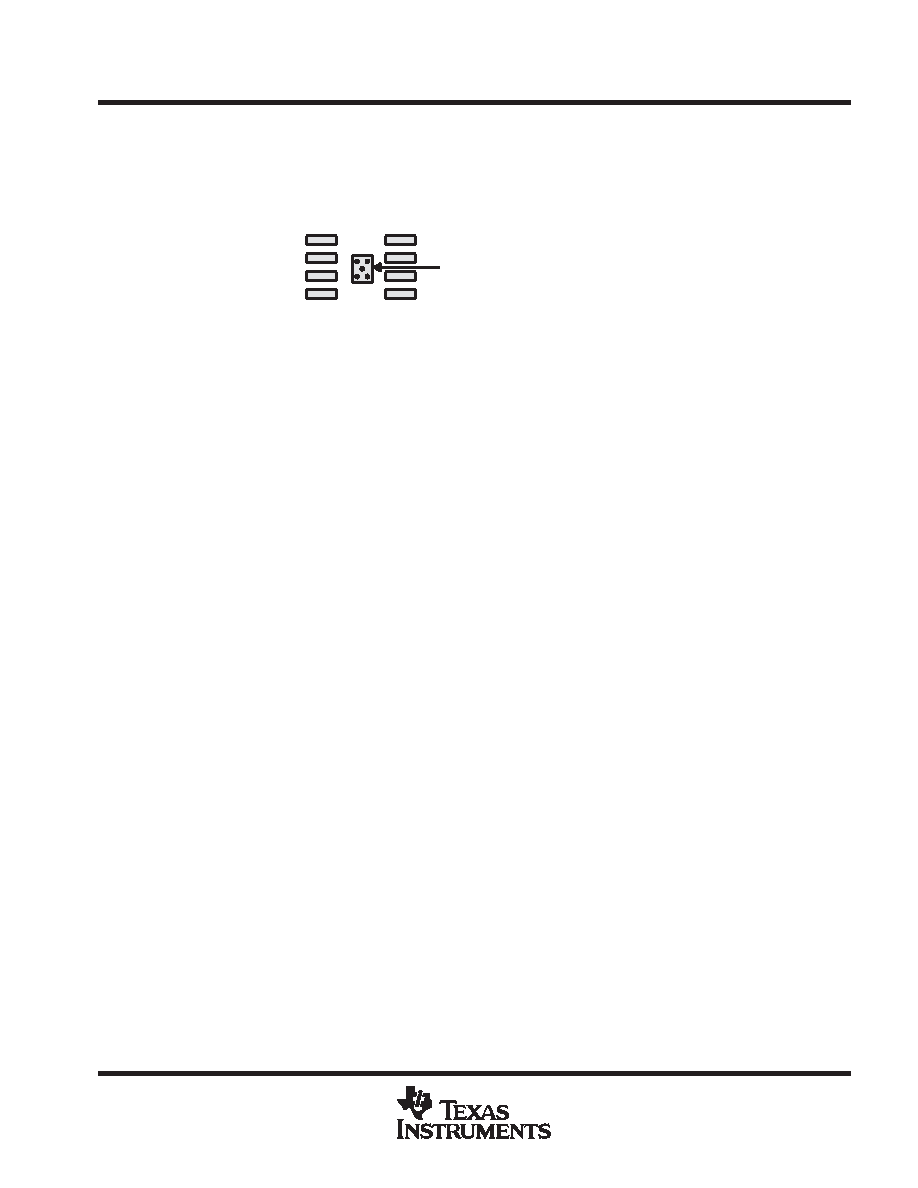
Thermal pad area (68 mils x 70 mils) with 5 vias
(Via diameter = 13 mils)
Figure 45. PowerPAD PCB Etch and Via Pattern
1.
Prepare the PCB with a top side etch pattern as shown in Figure 45. There should be etch for the leads as
well as etch for the thermal pad.
2.
Place five holes in the area of the thermal pad. These holes should be 13 mils in diameter. Keep them small
so that solder wicking through the holes is not a problem during reflow.
3.
Additional vias may be placed anywhere along the thermal plane outside of the thermal pad area. This helps
dissipate the heat generated by the THS408xDGN IC. These additional vias may be larger than the 13-mil
diameter vias directly under the thermal pad. They can be larger because they are not in the thermal pad
area to be soldered, so wicking is not a problem.
4.
Connect all holes to the internal ground plane.
5.
When connecting these holes to the ground plane, do not use the typical web or spoke via connection
methodology. Web connections have a high thermal resistance connection that is useful for slowing the heat
transfer during soldering operations. This makes the soldering of vias that have plane connections easier.
In this application, however, low thermal resistance is desired for the most efficient heat transfer. Therefore,
the holes under the THS408xDGN package should make their connection to the internal ground plane with
a complete connection around the entire circumference of the plated-through hole.
6.
The top-side solder mask should leave the terminals of the package and the thermal pad area with its five
holes exposed. The bottom-side solder mask should cover the five holes of the thermal pad area. This
prevents solder from being pulled away from the thermal pad area during the reflow process.
7.
Apply solder paste to the exposed thermal pad area and all of the IC terminals.
8.
With these preparatory steps in place, the THS408xDGN IC is simply placed in position and run through
the solder reflow operation as any standard surface-mount component. This results in a part that is properly
installed.
相关PDF资料 |
PDF描述 |
|---|---|
| THS4082CDG4 | 1 CHANNEL, VIDEO AMPLIFIER, PDSO8 |
| THS4082IDGNG4 | 1 CHANNEL, VIDEO AMPLIFIER, PDSO8 |
| THS4081IDRG4 | 1 CHANNEL, VIDEO AMPLIFIER, PDSO8 |
| THS4082CDGN | 1 CHANNEL, VIDEO AMPLIFIER, PDSO8 |
| THS4211DRB | 1 CHANNEL, VIDEO AMPLIFIER, PDSO8 |
相关代理商/技术参数 |
参数描述 |
|---|---|
| THS412 | 制造商:TI 制造商全称:Texas Instruments 功能描述:200MHz, CMOS OPERATIONAL AMPLIFIER WITH SHUTDOWN |
| THS4120 | 制造商:TI 制造商全称:Texas Instruments 功能描述:HIGH-SPEED FULLY DIFFERENTIAL I/O AMPLIFIERS |
| THS4120CD | 功能描述:特殊用途放大器 Fully Differential CMOS RoHS:否 制造商:Texas Instruments 通道数量:Single 共模抑制比(最小值): 输入补偿电压: 工作电源电压:3 V to 5.5 V 电源电流:5 mA 最大功率耗散: 最大工作温度:+ 70 C 最小工作温度:- 40 C 安装风格:SMD/SMT 封装 / 箱体:QFN-20 封装:Reel |
| THS4120CDG4 | 功能描述:特殊用途放大器 3.3V 100 MHz 43 V/us Fully Diff CMOS Amp RoHS:否 制造商:Texas Instruments 通道数量:Single 共模抑制比(最小值): 输入补偿电压: 工作电源电压:3 V to 5.5 V 电源电流:5 mA 最大功率耗散: 最大工作温度:+ 70 C 最小工作温度:- 40 C 安装风格:SMD/SMT 封装 / 箱体:QFN-20 封装:Reel |
| THS4120CDGK | 功能描述:特殊用途放大器 Fully Differential CMOS RoHS:否 制造商:Texas Instruments 通道数量:Single 共模抑制比(最小值): 输入补偿电压: 工作电源电压:3 V to 5.5 V 电源电流:5 mA 最大功率耗散: 最大工作温度:+ 70 C 最小工作温度:- 40 C 安装风格:SMD/SMT 封装 / 箱体:QFN-20 封装:Reel |
发布紧急采购,3分钟左右您将得到回复。