- 您现在的位置:买卖IC网 > PDF目录98229 > THS7319IZSVT (TEXAS INSTRUMENTS INC) 3 CHANNEL, VIDEO AMPLIFIER, PBGA9 PDF资料下载
参数资料
| 型号: | THS7319IZSVT |
| 厂商: | TEXAS INSTRUMENTS INC |
| 元件分类: | 音频/视频放大 |
| 英文描述: | 3 CHANNEL, VIDEO AMPLIFIER, PBGA9 |
| 封装: | 1.50 X 1.50 MM, 0.35 MM HEIGHT, GREEN, UCSP-9 |
| 文件页数: | 10/33页 |
| 文件大小: | 733K |
| 代理商: | THS7319IZSVT |
第1页第2页第3页第4页第5页第6页第7页第8页第9页当前第10页第11页第12页第13页第14页第15页第16页第17页第18页第19页第20页第21页第22页第23页第24页第25页第26页第27页第28页第29页第30页第31页第32页第33页
INPUT OPERATION
Level
Shift
Internal
Circuitry
+V
S
Input
Pin
SBOS468A – JUNE 2009 – REVISED JULY 2009.............................................................................................................................................................. www.ti.com
Because the internal gain is fixed at +6 dB (2 V/V), it
dictates the allowable linear input voltage range. For
The inputs to the THS7319 allow for dc-coupled
example, if the power supply is set to 3 V, the
inputs. Most DACs or video encoders can be
maximum output is approximately 2.9 V while driving
dc-connected to the THS7319 with essentially any
a significant amount of current. Thus, to avoid
DAC termination resistance desired for the system.
clipping, the allowable input is ([2.9 V – 0.15 V]/2) =
One of the potential drawbacks to dc-coupling is
1.375 V. This range is valid for up to the maximum
when 0 V is applied to the input from the DAC.
recommended
5-V
power
supply
that
allows
Although the input of the THS7319 allows for a 0-V
approximately a ([4.9 V – 0.15 V]/2) = 2.375 V input
input signal without issue, the output swing of a
range while avoiding clipping on the output.
traditional amplifier cannot yield a 0-V signal that
results in possible clipping of the signal. This
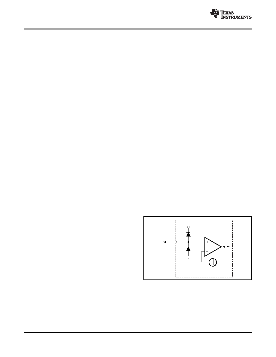
The input impedance of the THS7319 is dictated by
limitation is true for any single-supply amplifier
the internal high-impedance unity-gain buffer as
because
of
the
characteristics
of
the
output
shown in Figure 51. This buffer has a very high
transistors. Neither CMOS nor bipolar transistors can
2.4 M
|| 2 pF input impedance that is effectively
achieve 0 V while sinking current. This transistor
transparent to the source with no interactions. Unlike
characteristic is also the same reason why the
other products where the filter elements are tied
highest output voltage is always less than the
directly to the input pin without buffering, there are no
power-supply voltage when sourcing current.
filter performance changes or interaction with the
DAC termination resistance. Note that the internal
This output clipping can reduce the sync amplitudes
voltage shift does not appear at the input pin; it only
(both horizontal and vertical sync) on the video
shows at the output pin.
signal. A problem occurs if the video signal receiver
uses an automatic gain control (AGC) loop to account
While ac-coupling with dc-biasing using external
for losses in the transmission line. Some video AGC
resistor dividers can be done, it is generally not
circuits
derive
gain
from
the
horizontal
sync
recommended because of the large resistor values
amplitude. If clipping occurs on the sync amplitude,
required. These large resistor values coupled with the
then the AGC circuit can increase the gain too
input bias current of the THS7319 input can cause a
much—resulting in too much luma and/or chroma
significant voltage shift to appear on the input. If ac
amplitude gain correction. This correction may result
coupling is necessary for a system, several elements
in a picture with an overly bright display with too
must be taken into account for a proper design: the
much color saturation.
high-pass corner frequency (typically desired to be
about 2.5-Hz); the size of the input capacitor value;
Other AGC circuits may use the chroma burst
the parallel input resistance of the voltage divider;
amplitude for amplitude control. For this situation,
and the input bias current. Contact Texas Instruments
reduction in the sync signals does not alter the proper
for design support if ac coupling is necessary in the
gain setting. However, it is good engineering design
design.
practice to ensure that saturation/clipping does not
take place. Transistors always take a finite amount of
time to come out of saturation. This saturation could
possibly result in timing delays or other aberrations
on the signals that may not be desirable.
To eliminate saturation or clipping problems, the
THS7319 has a 150-mV output level shift feature.
This feature takes the input voltage and adds an
internal +75-mV shift to the input signal. Because of
the 6-dB (2 V/V) gain, the resulting output with a 0-V
applied input signal is approximately 150 mV. The
THS7319 rail-to-rail output stage can create this
output level while connected to a typical video load.
This configuration ensures the sync signal clipping or
saturation does not occur. This shift is constant,
Figure 51. Equivalent DC Input Mode Circuit
regardless of the input signal. The equation for this is
VOUT = (VIN × 2 V/V) + 0.15 V. For example, if a 1-V
input is applied, the output is (1 V × 2 V/V) + 0.15 V =
2.15 V.
18
Copyright 2009, Texas Instruments Incorporated
Product Folder Link(s): THS7319
相关PDF资料 |
PDF描述 |
|---|---|
| THS7360IPWR | VIDEO AMPLIFIER, PDSO20 |
| THS7360IPW | VIDEO AMPLIFIER, PDSO20 |
| THS7364IPWR | 6 CHANNEL, VIDEO AMPLIFIER, PDSO20 |
| THS7364IPW | 6 CHANNEL, VIDEO AMPLIFIER, PDSO20 |
| THS7365IPWR | 6 CHANNEL, VIDEO AMPLIFIER, PDSO20 |
相关代理商/技术参数 |
参数描述 |
|---|---|
| THS7320 | 制造商:TI 制造商全称:Texas Instruments 功能描述:3-Channel ED Filter Video Amplifier with 4-V/V Gain |
| THS7320IYHCR | 制造商:Texas Instruments 功能描述:3-CHANL ED FILTER VIDEO AMP, 4V/V GAIN - Tape and Reel 制造商:Texas Instruments 功能描述:IC 3-CH INTEG VIDEO AMP 9DSBGA 制造商:Texas Instruments 功能描述:Video Amplifiers 3-Ch ED Fltr Video Amp w/ 4V/V Gain 制造商:Texas Instruments 功能描述:3-Chanl ED Filter Video Amp, 4V/V Gain |
| THS7320IYHCT | 制造商:Texas Instruments 功能描述:IC 3-CH INTEG VIDEO AMP 9DSBGA |
| THS7320YHCEVM | 制造商:Texas Instruments 功能描述:THS7320YHCEVM - Boxed Product (Development Kits) 制造商:Texas Instruments 功能描述:Texas Instruments THS7320YHCEVM Development Kits 制造商:Texas Instruments 功能描述:MODULE EVAL FOR THS7320 ZSV 制造商:Texas Instruments 功能描述:EVAL BOARD, THS7320 VIDEO AMPLIFIER, Silicon Manufacturer:Texas Instruments, Silicon Core Number:THS7320, Kit Application Type:Amplifier, Application Sub Type:Video Buffer and Filter, Kit Contents:Eval Board THS7320 |
| THS7327 | 制造商:TI 制造商全称:Texas Instruments 功能描述:3-Channel RGBHV Video Buffer with I2C Control, Selectable Filters, Monitor Pass-Thru,2:1 Input MUX, and Selectable Input Bias Modes |
发布紧急采购,3分钟左右您将得到回复。