- 您现在的位置:买卖IC网 > PDF目录98230 > TK14489V (TOKO INC) FM, AUDIO SINGLE CHIP RECEIVER, PDSO20 PDF资料下载
参数资料
| 型号: | TK14489V |
| 厂商: | TOKO INC |
| 元件分类: | 接收器 |
| 英文描述: | FM, AUDIO SINGLE CHIP RECEIVER, PDSO20 |
| 封装: | TSSOP-20 |
| 文件页数: | 16/25页 |
| 文件大小: | 2570K |
| 代理商: | TK14489V |
TK14489V
GC3-E011E
Page 23
=
1
10
log
20
R
G
f
()
dB
(4)
Figure 14: Inverting OP Amp
R
1
R
f
V
IN
V
OUT
~
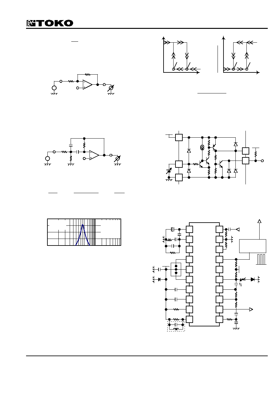
12-6-2. Active BPF
Examples of active BPF application as following draw in
fig. 15, and its frequency characteristics as following
draw in fig.16.
Figure 15: Active BPF
R
3
R
1
C
R
2
V
IN
V
OUT
~
Next expressions are formularized, however, G
0 is the
gain at center frequency f
0, and 3dB band width Q=f0/BW.
0
3
1
2G
R
=
,
3
1
2
3
1
2
4
R
Q
R
=
,
C
f
Q
R
0
3
π
=
(5)
Figure 16: Frequency Response
1k
Gain[dB]
0
20
15
10
5
100k
10k
R
1=18k
R
2=750
R
3=390k
C=0.001
F
V
CC=4.0V
V
in=50mV
f
in, Filter Amplifier Input Frequency[Hz]
12-7. Squelch
The output, which is controlled in accordance with noise
level from the rectifier, is injected into squelch input
terminal.
Squelch input has hysteresis to obstruct input jitter.
The threshold voltage and the hysteresis width are
variable
by
changing
hysteresis
resistor
RHYS
connecting with pin 18.
V
TH: Hi Threshold Voltage, VTH: Lo Threshold Voltage in
fig.17.
Figure 17: Squelch Response
i) Pin 13 Output
ii) Pin 14 Output
V
SQ[V]
V
TL
V
TH
Scan
Control
[V]
V
SQ[V]
V
TL
V
TH
Scan
Control
[V]
*V
TH: Hi Threshold Voltage, VTL: Lo Threshold Voltage
As Fig. 18 shows,
Scan Control (Pin 14) is "open
collector". So this pin operates normally if this is pulled
up the voltage which is over supply voltage but it's under
the maximum voltage.
Figure 18: Squelch
Vcc
12
14
13
4
15
V
SQ
Vcc2
12-8. FSK
A FSK application example is shown in fig.19.
Figure 19: FSK Application
Vcc
30k
50
0.01
F
430
1
F
100k
2.4k
V
CC
0V
DECORDER
Vcc
270pF
82pF
27.095
MHz
0.1
F
8.2k
1000pF
0.1
F
+
2.2
H
10
F
1
2
4
5
6
7
8
14
13
15
16
17
19
20
3
10
9
18
12
11
2k
1
F
RSSI
20k
270k
27.550
MHz
5.1k
47pF
7BRE-7437Z
22k
ALFC455G
0.1
F
Waveform-shaping of FSK demodulated signal is done
相关PDF资料 |
PDF描述 |
|---|---|
| TK15405BM | 1 CHANNEL, VIDEO AMPLIFIER, PDSO6 |
| TK15405BM | 1 CHANNEL, VIDEO AMPLIFIER, PDSO6 |
| TK15417BM | 1 CHANNEL, VIDEO AMPLIFIER, PDSO6 |
| TK15417BM | 1 CHANNEL, VIDEO AMPLIFIER, PDSO6 |
| TK15450L | 2 CHANNEL, VIDEO AMPLIFIER, PDSO8 |
相关代理商/技术参数 |
参数描述 |
|---|---|
| TK14551V | 制造商:TOKO 制造商全称:TOKO, Inc 功能描述:FM IF DETECTOR/AMPLIFIER |
| TK14551V/14551 | 制造商:TOKO 制造商全称:TOKO, Inc 功能描述:FM IF DETECTOR/AMPLIFIER |
| TK14551VTL | 制造商:TOKO 制造商全称:TOKO, Inc 功能描述:FM IF DETECTOR/AMPLIFIER |
| TK14552V | 制造商:TOKO 制造商全称:TOKO, Inc 功能描述:Wide band AM / ASK IF IC for ETC |
| TK14583V-G | 制造商:TOKO 制造商全称:TOKO, Inc 功能描述:Wide band FM IF IC for remote keyless entry / tire pressure monitoring system |
发布紧急采购,3分钟左右您将得到回复。