- 您现在的位置:买卖IC网 > PDF目录299979 > TK740SIL-2727 (TOKO INC) DUAL OUTPUT, FIXED POSITIVE LDO REGULATOR, PDSO8 PDF资料下载
参数资料
| 型号: | TK740SIL-2727 |
| 厂商: | TOKO INC |
| 元件分类: | 固定正电压多路输出LDO稳压器 |
| 英文描述: | DUAL OUTPUT, FIXED POSITIVE LDO REGULATOR, PDSO8 |
| 封装: | SOT-23, 8 PIN |
| 文件页数: | 14/29页 |
| 文件大小: | 584K |
| 代理商: | TK740SIL-2727 |
第1页第2页第3页第4页第5页第6页第7页第8页第9页第10页第11页第12页第13页当前第14页第15页第16页第17页第18页第19页第20页第21页第22页第23页第24页第25页第26页第27页第28页第29页
January 22, 2002 TOKO, Inc.
Page 21
TK740xxL
DEFINITION AND EXPLANATION OF TECHNICAL TERMS (CONT.)
PACKAGE POWER DISSIPATION (P
D)
This is the power dissipation level at which the thermal
sensor is activated. The IC contains an internal thermal
sensor which monitors the junction temperature. When the
junction temperature exceeds the monitor threshold of
150 °C, the IC is shut down. The junction temperature rises
as the difference between the input power (V
IN x IIN) and the
output power (V
OUT x IOUT) increases. The rate of tempera-
ture rise is greatly affected by the mounting pad configura-
tion on the PCB, the board material, and the ambient
temperature. When the IC mounting has good thermal
conductivity, the junction temperature will be low even if the
power dissipation is large. When mounted on the recom-
mended mounting pad, the power dissipation of the
SOT23L-8 is increased to 600 mW. For operation at
ambient temperatures over 25 °C, the power dissipation of
the SOT23L-8 device should be derated at 4.8 mW/ °C. To
determine the power dissipation for shutdown when mounted,
attach the device on the actual PCB and deliberately
increase the output current (or raise the input voltage) until
the thermal protection circuit is activated. Calculate the
power dissipation of the device by subtracting the output
power from the input power. These measurements should
allow for the ambient temperature of the PCB. The value
obtained from P
D /(150 °C - TA) is the derating factor. The
PCB mounting pad should provide maximum thermal con-
ductivity in order to maintain low device temperatures. As
a general rule, the lower the temperature, the better the
reliability of the device. The thermal resistance when
mounted is expressed as follows:
T
j = 0jA x PD + TA
For Toko ICs, the internal limit for junction temperature is
150 °C. If the ambient temperature (T
A) is 25 °C, then:
150 °C = 0
jA x PD + 25 °C
0
jA = 125 °C / PD
0
jA = 125 °C / PD (°C / mW)
P
D is the value when the thermal protection circuit is
activated. A simple way to determine P
D is to calculate VIN
x I
IN when the output side is shorted. Input current gradually
falls as temperature rises. You should use the value when
thermal equilibrium is reached.
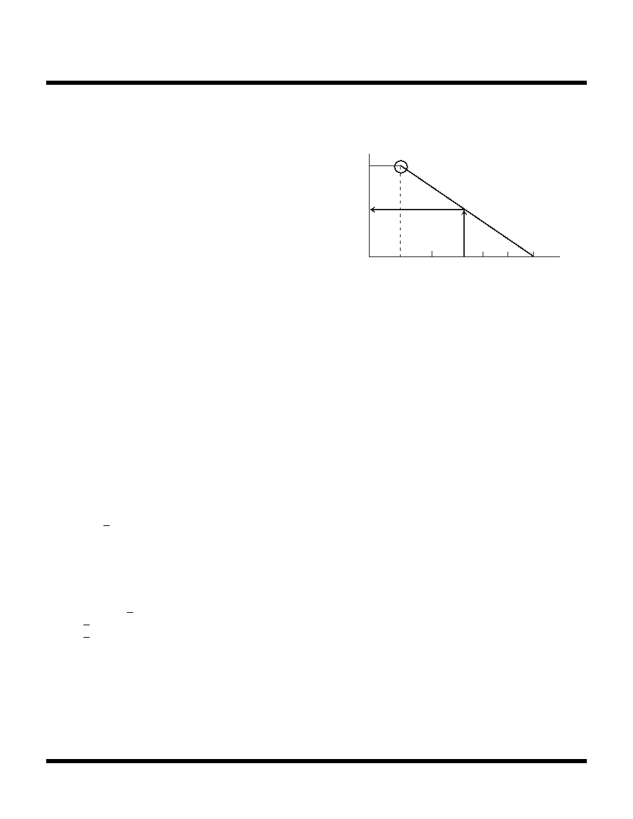
The range of usable currents can also be found from the
graph below.
Procedure:
1) Find P
D
2) P
D1 is taken to be PD x (~0.8 - 0.9)
3) Plot P
D1 against 25 °C
4) Connect P
D1 to the point corresponding to the 150 °C with
a straight line.
5)
In design, take a vertical line from the maximum
operating temperature (e.g., 75 °C) to the derating curve.
6) Read off the value of P
D against the point at which the
vertical line intersects the derating curve. This is taken as
the maximum power dissipation, D
PD.
The maximum operating current is:
I
OUT = (DPD / (VIN(MAX) - VOUT)
Pd
25
50
75
150
TA (°C)
3
PD(mW)
5
0
100
2
4
相关PDF资料 |
PDF描述 |
|---|---|
| TL12W03-L(T30) | SINGLE COLOR LED, WARM WHITE |
| TL6700AF160QJ | KEYPAD SWITCH, SPST, MOMENTARY, 0.05A, 12VDC, 2.06 N, SURFACE MOUNT-STRAIGHT |
| TL750M05CKTE | 5 V FIXED POSITIVE LDO REGULATOR, 0.6 V DROPOUT, PSSO3 |
| TL750M05Y | 5 V FIXED POSITIVE LDO REGULATOR, 0.6 V DROPOUT, UUC3 |
| TL751M12QKC | 12 V FIXED POSITIVE LDO REGULATOR, 0.6 V DROPOUT, PSFM5 |
相关代理商/技术参数 |
参数描述 |
|---|---|
| TK75 | 制造商:ALTECH 制造商全称:Altech corporation 功能描述:POLYCARBONATE ENCLOSURE TK 75 |
| TK7500 | 功能描述:冲压机与冲模 FRM W/4 DIES & CASE RoHS:否 制造商:Souriau 大小: 产品:Dies 类型:Crimping 描述/功能: |
| TK75001 | 制造商:TOKO 制造商全称:TOKO, Inc 功能描述:PWM CONTROLLER |
| TK75001D | 制造商:TOKO 制造商全称:TOKO, Inc 功能描述:PWM CONTROLLER |
| TK75001DIMG | 制造商:TOKO 制造商全称:TOKO, Inc 功能描述:PWM CONTROLLER |
发布紧急采购,3分钟左右您将得到回复。