- 您现在的位置:买卖IC网 > PDF目录69490 > TL441CNSR (TEXAS INSTRUMENTS INC) DUAL LOG OR ANTILOG AMPLIFIER, 40 MHz BAND WIDTH, PDSO16 PDF资料下载
参数资料
| 型号: | TL441CNSR |
| 厂商: | TEXAS INSTRUMENTS INC |
| 元件分类: | 模拟运算功能 |
| 英文描述: | DUAL LOG OR ANTILOG AMPLIFIER, 40 MHz BAND WIDTH, PDSO16 |
| 封装: | GREEN, PLASTIC, SOP-16 |
| 文件页数: | 19/20页 |
| 文件大小: | 557K |
| 代理商: | TL441CNSR |
TL441
LOGARITHMIC AMPLIFIER
SLVS328 – OCTOBER 2000
8
POST OFFICE BOX 655303
DALLAS, TEXAS 75265
APPLICATION INFORMATION
Although designed for high-performance applications such as infrared detection, this device has a wide range
of applications in data compression and analog computation.
basic logarithmic function
The basic logarithmic response is derived from
the exponential current-voltage relationship of
collector current and base-emitter voltage. This
relationship is given in the equation:
m
VBE = In [(IC + ICES)/ICES]
where:
IC = collector current
ICES = collector current at VBE = 0
m =
q/kT (in V – 1)
VBE = base-emitter voltage
The differential input amplifier allows dual-polarity
inputs, is self-compensating for temperature
variations,
and
is
relatively
insensitive
to
common-mode noise.
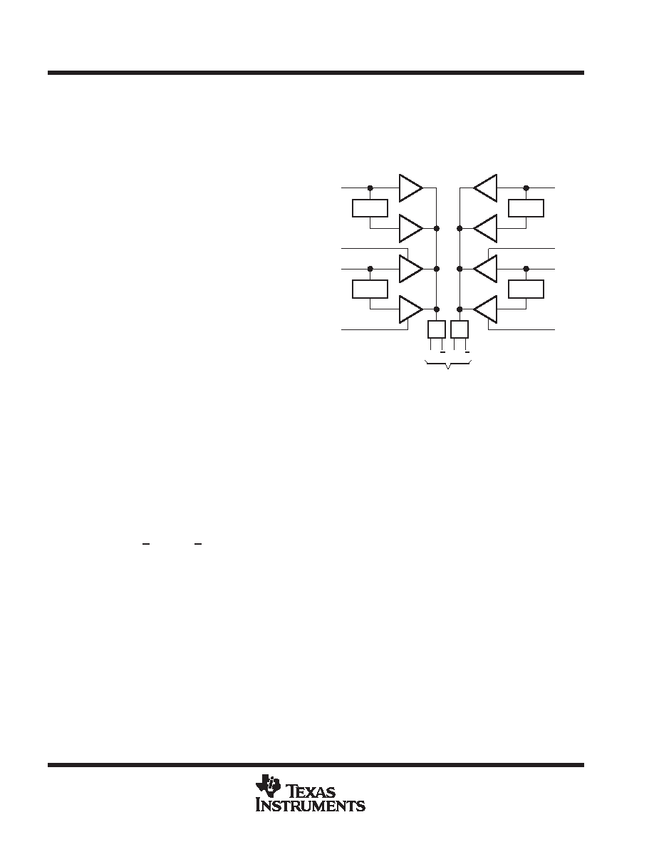
logarithmic sections
As can be seen from the schematic, there are eight differential pairs. Each pair is a 15-dB log subsection, and
each input feeds two pairs, for a range of 30-dB per stage.
Four compensation points are available to allow slight variations in the gain (slope) of the two individual 15-dB
stages of input A2 and B2. By slightly changing the voltage on any of the compensation pins from their quiescent
values, the gain of that particular 15-dB stage can be adjusted to match the other 15-dB stage in the pair. The
compensation pins also can be used to match the transfer characteristics of input A2 to A1 or B2 to B1.
The log stages in each half of the circuit are summed by directly connecting their collectors together and
summing through a common-base output stage. The two sets of output collectors are used to give two log
outputs, Y and Y (or Z and Z), which are equal in amplitude, but opposite in polarity. This increases the versatility
of the device.
By proper choice of external connections, linear amplification, and linear attenuation, and many different
applications requiring logarithmic signal processing are possible
input levels
The recommended input voltage range of any one stage is given as 0.01 V to 1 V. Input levels in excess of
1 V may result in a distorted output. When several log sections are summed together, the distorted area of one
section overlaps with the next section and the resulting distortion is insignificant. However, there is a limit to the
amount of overdrive that can be applied. As the input drive reaches
±3.5 V, saturation occurs, clamping the
collector-summing line and severely distorting the output. Therefore, the signal to any input must be limited to
approximately
±3 V to ensure a clean output.
Figure 10
INPUT
A1
CA2
INPUT
A2
CA2’
Log
–15 dB
ΣΣ
YY
Z
Outputs
INPUT
B1
CB2
INPUT
B2
CB2’
functional block diagram
相关PDF资料 |
PDF描述 |
|---|---|
| TL494CDB | 0.25 A SWITCHING CONTROLLER, 300 kHz SWITCHING FREQ-MAX, PDSO16 |
| TL494CNSE4 | 0.25 A SWITCHING CONTROLLER, 300 kHz SWITCHING FREQ-MAX, PDSO16 |
| TL494CPWG4 | 0.25 A SWITCHING CONTROLLER, 300 kHz SWITCHING FREQ-MAX, PDSO16 |
| TL494CPW | 0.25 A SWITCHING CONTROLLER, 300 kHz SWITCHING FREQ-MAX, PDSO16 |
| TL494MJ | 0.25 A SWITCHING CONTROLLER, 300 kHz SWITCHING FREQ-MAX, CDIP16 |
相关代理商/技术参数 |
参数描述 |
|---|---|
| TL441CNSRE4 | 功能描述:对数放大器 LOGARITHMIC AMP RoHS:否 制造商:Texas Instruments 通道数量:3 带宽:3 dB 共模抑制比(最小值): 输入补偿电压:+/- 7 mV 输入电压范围(最大值):5.5 V 工作电源电压:4.5 V to 5.5 V 电源电流:+/- 15 mA 工作温度范围:- 40 C to +85 C 安装风格:SMD/SMT 封装 / 箱体:VQFN-16 封装:Reel |
| TL441CNSRG4 | 功能描述:对数放大器 Logarithmic Amp RoHS:否 制造商:Texas Instruments 通道数量:3 带宽:3 dB 共模抑制比(最小值): 输入补偿电压:+/- 7 mV 输入电压范围(最大值):5.5 V 工作电源电压:4.5 V to 5.5 V 电源电流:+/- 15 mA 工作温度范围:- 40 C to +85 C 安装风格:SMD/SMT 封装 / 箱体:VQFN-16 封装:Reel |
| TL441-EP | 制造商:TI 制造商全称:Texas Instruments 功能描述:LOGARITHMIC AMPLIFIER |
| TL441MNSREP | 功能描述:对数放大器 Mil Enhance Logar Amp RoHS:否 制造商:Texas Instruments 通道数量:3 带宽:3 dB 共模抑制比(最小值): 输入补偿电压:+/- 7 mV 输入电压范围(最大值):5.5 V 工作电源电压:4.5 V to 5.5 V 电源电流:+/- 15 mA 工作温度范围:- 40 C to +85 C 安装风格:SMD/SMT 封装 / 箱体:VQFN-16 封装:Reel |
| TL441N | 制造商:TI 制造商全称:Texas Instruments 功能描述:LOGARITHMIC AMPLIFIER |
发布紧急采购,3分钟左右您将得到回复。