- 您现在的位置:买卖IC网 > PDF目录98231 > TL592BPSRE4 (TEXAS INSTRUMENTS INC) 1 CHANNEL, VIDEO AMPLIFIER, PDSO8 PDF资料下载
参数资料
| 型号: | TL592BPSRE4 |
| 厂商: | TEXAS INSTRUMENTS INC |
| 元件分类: | 音频/视频放大 |
| 英文描述: | 1 CHANNEL, VIDEO AMPLIFIER, PDSO8 |
| 封装: | GREEN, PLASTIC, SOP-8 |
| 文件页数: | 7/14页 |
| 文件大小: | 511K |
| 代理商: | TL592BPSRE4 |
1
8
2
IN+
IN–
B
A
7
Gain
Adjust
6
4
5
3
V
CC+
V
CC–
OUT+
OUT–
ABSOLUTE MAXIMUM RATINGS
(1) (2)
DISSIPATION RATINGS
SLFS001B – JUNE 1985 – REVISED APRIL 2008 ............................................................................................................................................................. www.ti.com
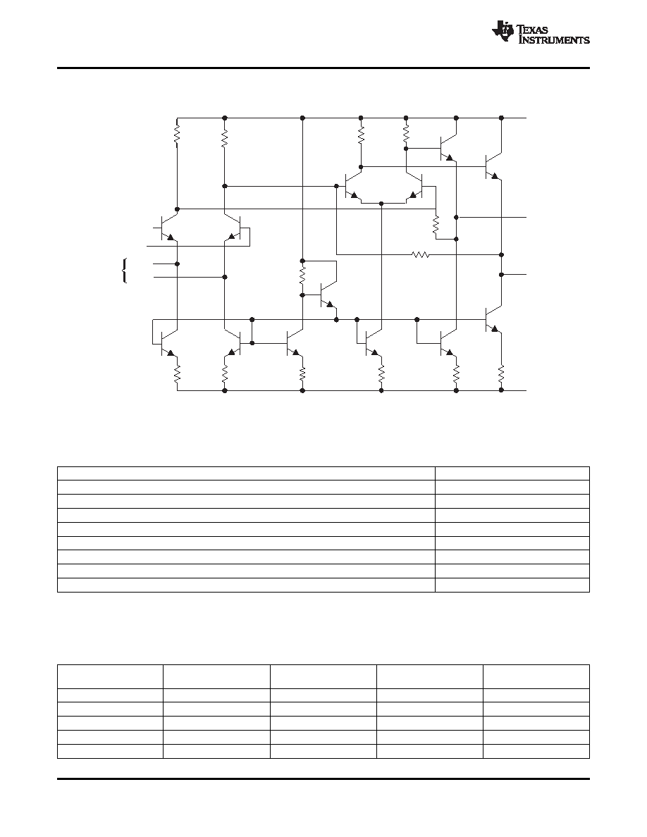
SCHEMATIC
NOTE: Pin numbers shown are for D, P, and PS packages.
over operating free-air temperature range (unless otherwise noted)
VCC+
Positive supply voltage
8 V
VCC–
Negative supply voltage
–8 V
VDI
Differential input voltage
±5 V
VI
Voltage range, any input
VCC+ to VCC–
IO
Output current
10 mA
PD
Continuous total power dissipation
See Dissipation Rating Table
TA
Operating free-air temperature range
0
°C to 70°C
Tstg
Storage temperature range
–65
°C to 150°C
Tlead
Lead temperature 1,6 mm (1/16 inch) from case for 10 seconds
260
°C
(1)
Stresses beyond those listed under absolute maximum ratings may cause permanent damage to the device. These are stress ratings
only, and functional operation of the device at these or any other conditions beyond those indicated under recommended operating
conditions is not implied. Exposure to absolute-maximum-rated conditions for extended periods may affect device reliability.
(2)
All voltage values except differential input voltages are with respect to the midpoint between VCC+ and VCC–.
TA ≤ 25°C
TA = 70°C
PACKAGE
DERATING FACTOR
DERATE ABOVE TA
POWER RATING
D8
530 mW
5.8 mW/
°C
59
464 mW
D14
530 mW
N/A
530 mW
N
530 mW
N/A
530 mW
P
530 mW
N/A
530 mW
PS
530 mW
N/A
530 mW
2
Copyright 1985–2008, Texas Instruments Incorporated
Product Folder Link(s): TL592B
相关PDF资料 |
PDF描述 |
|---|---|
| TL592BPE4 | 1 CHANNEL, VIDEO AMPLIFIER, PDIP8 |
| TL7700CPSE4 | 1-CHANNEL POWER SUPPLY SUPPORT CKT, PDSO8 |
| TL7705ACPSE4 | 1-CHANNEL POWER SUPPLY SUPPORT CKT, PDSO8 |
| TL7705AID1/A | 1-CHANNEL POWER SUPPLY SUPPORT CKT, PDSO8 |
| TL7709ACY | 1-CHANNEL POWER SUPPLY SUPPORT CKT, UUC8 |
相关代理商/技术参数 |
参数描述 |
|---|---|
| TL592BPSRG4 | 功能描述:视频放大器 Differential Video Amp RoHS:否 制造商:ON Semiconductor 通道数量:4 电源类型: 工作电源电压:3.3 V, 5 V 电源电流: 最小工作温度: 最大工作温度: 封装 / 箱体:TSSOP-14 封装:Reel |
| TL592CD | 制造商:Texas Instruments 功能描述:592CD |
| TL592P | 制造商:Texas Instruments 功能描述: |
| TL592PS | 制造商:Texas Instruments 功能描述: |
| TL-5930 | 制造商:Tadiran Batteries 功能描述:BATTERY |
发布紧急采购,3分钟左右您将得到回复。