- 您现在的位置:买卖IC网 > PDF目录150821 > TL7726QDRG4 (TEXAS INSTRUMENTS INC) SPECIALTY ANALOG CIRCUIT, PDSO8 PDF资料下载
参数资料
| 型号: | TL7726QDRG4 |
| 厂商: | TEXAS INSTRUMENTS INC |
| 元件分类: | 模拟信号调理 |
| 英文描述: | SPECIALTY ANALOG CIRCUIT, PDSO8 |
| 封装: | GREEN, PLASTIC, MS-012AA, SOIC-8 |
| 文件页数: | 5/12页 |
| 文件大小: | 407K |
| 代理商: | TL7726QDRG4 |
TL7726
HEX CLAMPING CIRCUITS
SLAS078C – SEPTEMBER 1993 – REVISED JULY 1999
2
POST OFFICE BOX 655303
DALLAS, TEXAS 75265
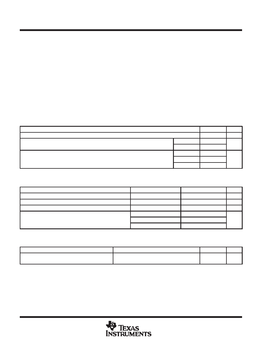
absolute maximum ratings over operating free-air temperature (unless otherwise noted)
Reference voltage, Vref
6 V
. . . . . . . . . . . . . . . . . . . . . . . . . . . . . . . . . . . . . . . . . . . . . . . . . . . . . . . . . . . . . . . . . . . . . .
Clamping current, IIK
±50 mA
. . . . . . . . . . . . . . . . . . . . . . . . . . . . . . . . . . . . . . . . . . . . . . . . . . . . . . . . . . . . . . . . . . . .
Junction temperature, TJ
150
°C
. . . . . . . . . . . . . . . . . . . . . . . . . . . . . . . . . . . . . . . . . . . . . . . . . . . . . . . . . . . . . . . . . .
Package thermal impedance,
θJA (see Notes 1 and 2): D package
97
°C/W
. . . . . . . . . . . . . . . . . . . . . . . . . . . .
P package
127
°C/W
. . . . . . . . . . . . . . . . . . . . . . . . . . . .
Lead temperature 1,6 mm (1/16 inch) from case for 10 seconds
260
°C
. . . . . . . . . . . . . . . . . . . . . . . . . . . . . . .
Storage temperature range, Tstg
–65
°C to 150°C
. . . . . . . . . . . . . . . . . . . . . . . . . . . . . . . . . . . . . . . . . . . . . . . . . . .
Stresses beyond those listed under “absolute maximum ratings” may cause permanent damage to the device. These are stress ratings only, and
functional operation of the device at these or any other conditions beyond those indicated under “recommended operating conditions” is not
implied. Exposure to absolute-maximum-rated conditions for extended periods may affect device reliability.
NOTES:
1. Maximum power dissipation is a function of TJ(max), θJA, and TA. The maximum allowable power dissipation at any allowable
ambient temperature is PD = (TJ(max) – TA)/θJA. Operating at the absolute maximum TJ of 150°C can impact reliability.
2. The package thermal impedance is calculated in accordance with JESD 51, except for through-hole packages, which use a trace
length of zero.
recommended operating conditions
MIN
MAX
UNIT
Reference voltage, Vref
4.5
5.5
V
Input clamping current IIK
VI ≥ Vref
25
mA
Input clamping current, IIK
VI ≤ GND
–25
mA
TL7726C
0
70
Operating free-air temperature range, TA
TL7726I
–40
85
°C
TL7726Q
–40
125
electrical characteristics over recommended operating free-air temperature range (unless
otherwise noted)
PARAMETER
TEST CONDITIONS
MIN
TYP
MAX
UNIT
VIK +
Positive clamp voltage
II = 20 mA
Vref
Vref + 200
mV
VIK –
Negative clamp voltage
II = 20 mA
– 200
0
mV
IZ
Reference current
Vref = 5 V
25
60
A
Vref – 50 mV ≤ VI ≤ Vref
10
II
Input current
GND
≤ VI ≤ 50 mV
–10
A
50 mV
≤ VI ≤ Vref – 50 mV
–1
1
All typical values are at TA = 25°C.
switching characteristics specified at TA = 25°C
PARAMETER
TEST CONDITIONS
MIN
MAX
UNIT
t
Settling time
VI(system) = ±13 V,
RI = 600 ,
tt < 1 s,
30
s
ts
Settling time
I(system)
,
Measured at 10% to 90%,
I
,
See Figure 1
t
,
30
s
相关PDF资料 |
PDF描述 |
|---|---|
| TC1028CUA723 | SPECIALTY ANALOG CIRCUIT, PDSO8 |
| TPS61105PW | SWITCHING REGULATOR, 800 kHz SWITCHING FREQ-MAX, PDSO20 |
| TXS100ZB-NR2V | 1-OUTPUT 180 W DC-DC REG PWR SUPPLY MODULE |
| TXS100ZB-P2R3V | 1-OUTPUT 180 W DC-DC REG PWR SUPPLY MODULE |
| TXS100ZD-NP23H | 1-OUTPUT 250 W DC-DC REG PWR SUPPLY MODULE |
相关代理商/技术参数 |
参数描述 |
|---|---|
| TL7726QP | 功能描述:基准电压& 基准电流 HEX CLAMPING CIRCUIT RoHS:否 制造商:STMicroelectronics 产品:Voltage References 拓扑结构:Shunt References 参考类型:Programmable 输出电压:1.24 V to 18 V 初始准确度:0.25 % 平均温度系数(典型值):100 PPM / C 串联 VREF - 输入电压(最大值): 串联 VREF - 输入电压(最小值): 分流电流(最大值):60 mA 最大工作温度:+ 125 C 封装 / 箱体:SOT-23-3L 封装:Reel |
| TL77-2F-10 | 制造商:DBLECTRO 制造商全称:DB Lectro Inc 功能描述:PCB PLUG-IN TRANSFORMER |
| TL77-2F-12 | 制造商:DBLECTRO 制造商全称:DB Lectro Inc 功能描述:PCB PLUG-IN TRANSFORMER |
| TL77-2F-120 | 制造商:DBLECTRO 制造商全称:DB Lectro Inc 功能描述:PCB PLUG-IN TRANSFORMER |
| TL77-2F-16 | 制造商:DBLECTRO 制造商全称:DB Lectro Inc 功能描述:PCB PLUG-IN TRANSFORMER |
发布紧急采购,3分钟左右您将得到回复。