- 您现在的位置:买卖IC网 > PDF目录382602 > TLC075IDG4 (Texas Instruments, Inc.) FAMILY OF WIDE-BANDWIDTH HIGH-OUTPUT-DRIVE SINGLE SUPPLY OPERATIONAL AMPLIFIERS PDF资料下载
参数资料
| 型号: | TLC075IDG4 |
| 厂商: | Texas Instruments, Inc. |
| 英文描述: | FAMILY OF WIDE-BANDWIDTH HIGH-OUTPUT-DRIVE SINGLE SUPPLY OPERATIONAL AMPLIFIERS |
| 中文描述: | 家庭具有宽带高输出驱动单电源运算放大器 |
| 文件页数: | 22/50页 |
| 文件大小: | 1454K |
| 代理商: | TLC075IDG4 |
第1页第2页第3页第4页第5页第6页第7页第8页第9页第10页第11页第12页第13页第14页第15页第16页第17页第18页第19页第20页第21页当前第22页第23页第24页第25页第26页第27页第28页第29页第30页第31页第32页第33页第34页第35页第36页第37页第38页第39页第40页第41页第42页第43页第44页第45页第46页第47页第48页第49页第50页
SLOS219D JUNE 1999 REVISED FEBRUARY 2004
22
POST OFFICE BOX 14WWW.TI.COM
HOUSTON, TEXAS 772511443
APPLICATION INFORMATION
general PowerPAD design considerations
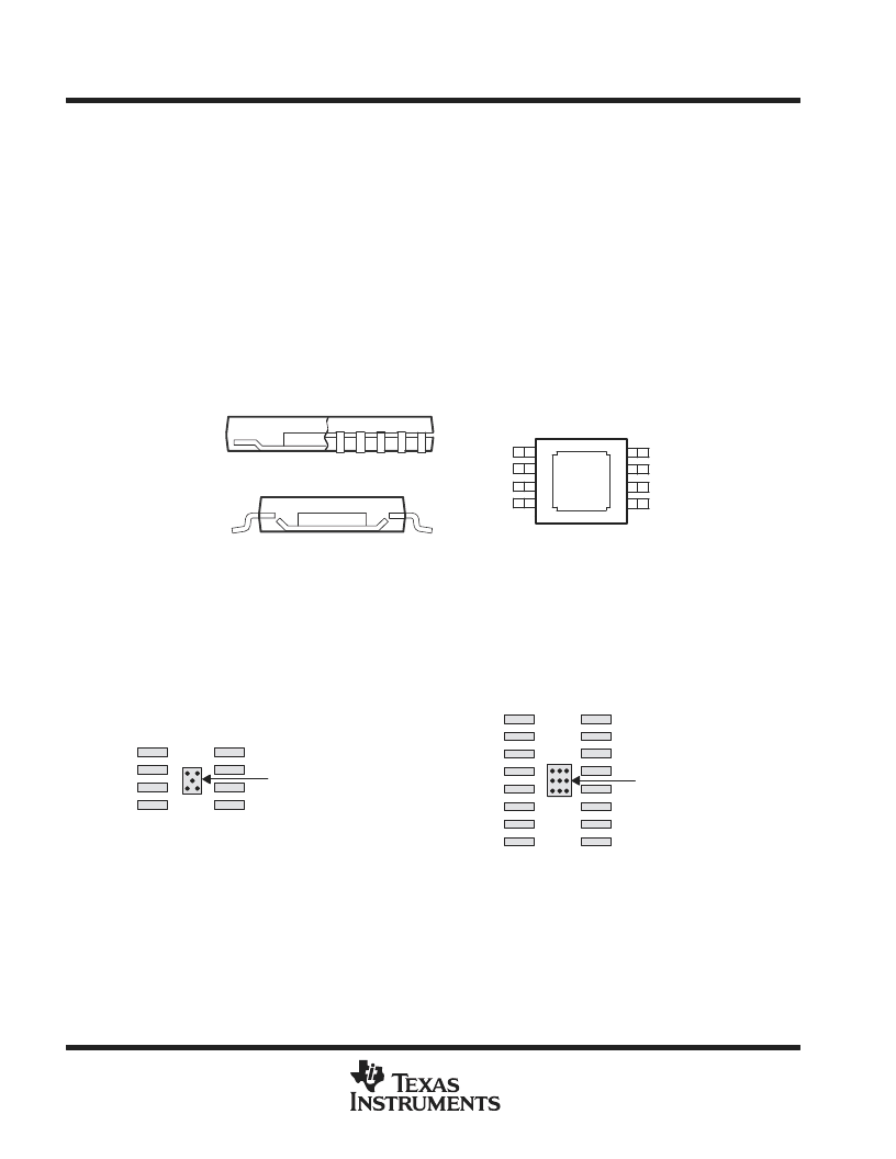
The TLC07x is available in a thermally-enhanced PowerPAD family of packages. These packages are
constructed using a downset leadframe upon which the die is mounted [see Figure 52(a) and Figure 52(b)]. This
arrangement results in the lead frame being exposed as a thermal pad on the underside of the package [see
Figure 52(c)]. Because this thermal pad has direct thermal contact with the die, excellent thermal performance
can be achieved by providing a good thermal path away from the thermal pad.
The PowerPAD package allows for both assembly and thermal management in one manufacturing operation.
During the surface-mount solder operation (when the leads are being soldered), the thermal pad can also be
soldered to a copper area underneath the package. Through the use of thermal paths within this copper area,
heat can be conducted away from the package into either a ground plane or other heat dissipating device.
The PowerPAD package represents a breakthrough in combining the small area and ease of assembly of
surface mount with the, heretofore, awkward mechanical methods of heatsinking.
DIE
Side View (a)
End View (b)
Bottom View (c)
DIE
Thermal
Pad
NOTE A: The thermal pad is electrically isolated from all terminals in the package.
Figure 52. Views of Thermally Enhanced DGN Package
Although there are many ways to properly heatsink the PowerPAD package, the following steps illustrate the
recommended approach.
68 mils x 70 mils with 5 vias
(Via diameter = 13 mils)
78 mils x 94 mils with 9 vias
(Via diameter = 13 mils)
Thermal Pad Area
Single or Dual
Quad
Figure 53. PowerPAD PCB Etch and Via Pattern
相关PDF资料 |
PDF描述 |
|---|---|
| TLC070CPE4 | FAMILY OF WIDE-BANDWIDTH HIGH-OUTPUT-DRIVE SINGLE SUPPLY OPERATIONAL AMPLIFIERS |
| TLC070IDGNG4 | FAMILY OF WIDE-BANDWIDTH HIGH-OUTPUT-DRIVE SINGLE SUPPLY OPERATIONAL AMPLIFIERS |
| TLC073ID | FAMILY OF WIDE-BANDWIDTH HIGH-OUTPUT-DRIVE SINGLE SUPPLY OPERATIONAL AMPLIFIERS |
| TLC075IDR | FAMILY OF WIDE-BANDWIDTH HIGH-OUTPUT-DRIVE SINGLE SUPPLY OPERATIONAL AMPLIFIERS |
| TLC075IDRG4 | FAMILY OF WIDE-BANDWIDTH HIGH-OUTPUT-DRIVE SINGLE SUPPLY OPERATIONAL AMPLIFIERS |
相关代理商/技术参数 |
参数描述 |
|---|---|
| TLC075IDR | 功能描述:运算放大器 - 运放 Quad Wide-Bandwidth Hi-Output-Drive RoHS:否 制造商:STMicroelectronics 通道数量:4 共模抑制比(最小值):63 dB 输入补偿电压:1 mV 输入偏流(最大值):10 pA 工作电源电压:2.7 V to 5.5 V 安装风格:SMD/SMT 封装 / 箱体:QFN-16 转换速度:0.89 V/us 关闭:No 输出电流:55 mA 最大工作温度:+ 125 C 封装:Reel |
| TLC075IDRG4 | 功能描述:运算放大器 - 运放 Quad Wide Bandwidth Op Amp w/Shutdown RoHS:否 制造商:STMicroelectronics 通道数量:4 共模抑制比(最小值):63 dB 输入补偿电压:1 mV 输入偏流(最大值):10 pA 工作电源电压:2.7 V to 5.5 V 安装风格:SMD/SMT 封装 / 箱体:QFN-16 转换速度:0.89 V/us 关闭:No 输出电流:55 mA 最大工作温度:+ 125 C 封装:Reel |
| TLC075IN | 功能描述:运算放大器 - 运放 Quad R/R RoHS:否 制造商:STMicroelectronics 通道数量:4 共模抑制比(最小值):63 dB 输入补偿电压:1 mV 输入偏流(最大值):10 pA 工作电源电压:2.7 V to 5.5 V 安装风格:SMD/SMT 封装 / 箱体:QFN-16 转换速度:0.89 V/us 关闭:No 输出电流:55 mA 最大工作温度:+ 125 C 封装:Reel |
| TLC075INE4 | 功能描述:运算放大器 - 运放 Quad Wide-Bandwidth Hi-Output-Drive RoHS:否 制造商:STMicroelectronics 通道数量:4 共模抑制比(最小值):63 dB 输入补偿电压:1 mV 输入偏流(最大值):10 pA 工作电源电压:2.7 V to 5.5 V 安装风格:SMD/SMT 封装 / 箱体:QFN-16 转换速度:0.89 V/us 关闭:No 输出电流:55 mA 最大工作温度:+ 125 C 封装:Reel |
| TLC075IPWP | 功能描述:运算放大器 - 运放 Quad High-Output RoHS:否 制造商:STMicroelectronics 通道数量:4 共模抑制比(最小值):63 dB 输入补偿电压:1 mV 输入偏流(最大值):10 pA 工作电源电压:2.7 V to 5.5 V 安装风格:SMD/SMT 封装 / 箱体:QFN-16 转换速度:0.89 V/us 关闭:No 输出电流:55 mA 最大工作温度:+ 125 C 封装:Reel |
发布紧急采购,3分钟左右您将得到回复。