- 您现在的位置:买卖IC网 > PDF目录67330 > TLC1543IDWR (TEXAS INSTRUMENTS INC) 11-CH 10-BIT SUCCESSIVE APPROXIMATION ADC, SERIAL ACCESS, PDSO20 PDF资料下载
参数资料
| 型号: | TLC1543IDWR |
| 厂商: | TEXAS INSTRUMENTS INC |
| 元件分类: | ADC |
| 英文描述: | 11-CH 10-BIT SUCCESSIVE APPROXIMATION ADC, SERIAL ACCESS, PDSO20 |
| 封装: | GREEN, PLASTIC, SOIC-20 |
| 文件页数: | 31/32页 |
| 文件大小: | 770K |
| 代理商: | TLC1543IDWR |
第1页第2页第3页第4页第5页第6页第7页第8页第9页第10页第11页第12页第13页第14页第15页第16页第17页第18页第19页第20页第21页第22页第23页第24页第25页第26页第27页第28页第29页第30页当前第31页第32页
www.ti.com
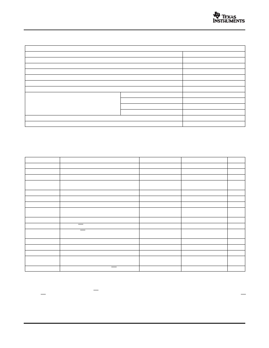
ABSOLUTE MAXIMUM RATINGS
RECOMMENDED OPERATING CONDITIONS
SLAS052G – MARCH 1992 – REVISED JANUARY 2006
over operating free-air temperature range (unless otherwise noted)(1)
UNIT
VCC, see (2)
Supply voltage range
-0.5 V to 6.5 V
VI
Input voltage range
-0.3 V to VCC + 0.3 V
VO
Output voltage range
-0.3 V to VCC + 0.3 V
Vref+
Positive reference voltage
VCC + 0.1 V
Vref-
Negative reference voltage
-0.1 V
Peak input current (any input)
±20 mA
Peak total input current (all inputs)
±30 mA
TLC1542C, TLC1543C
0
°C to 70°C
TLC1542I, TLC1543I
-40
°C to 85°C
TA
Operating free-air temperature range
TLC1542Q, TLC1543Q
-40
°C to 125°C
TLC1542M
-55
°C to 125°C
Tstg
Storage temperature range,
-65
°C to 150°C
Lead temperature 1,6 mm (1/16 inch) from the case for 10 seconds
260
°C
(1)
Stresses beyond those listed under absolute maximum ratings may cause permanent damage to the device. These are stress ratings
only, and functional operation of the device at these or any other conditions beyond those indicated under recommended operating
conditions is not implied. Exposure to absolute-maximum-rated conditions for extended periods may affect device reliability.
(2)
All voltage values are with respect to digital ground with REF- and GND wired together (unless otherwise noted).
MIN
NOM
MAX
UNIT
VCC
Supply voltage
4.5
5
5.5
V
Vref+, see(1)
Positive reference voltage
VCC
V
Vref-, see (1)
Negative reference voltage
0
V
VCC+0.
Vref+-Vref-, see (1)
Differential reference voltage
2.5
VCC
V
2
Analog input voltage ,see (1)
0
VCC
V
VIH
High-level control input voltage
VCC = 4.5 V to 5.5 V
2
V
VIL
Low-level control input voltage
VCC = 4.5 V to 5.5 V
0.8
V
Setup time, address bits at data input before I/O
100
ns
CLOCK
↑
Hold time, address bits after I/O CLOCK
↑
0
ns
Hold time, CS low after last I/O CLOCK
↓
0
ns
tsu(CS), see (2) and
Setup time, CS low before clocking in first
1.425
s
address bit
Clock frequency at I/O CLOCK, see (3)
0
2.1
MHz
twH(I/O)
Pulse duration, I/O CLOCK high,
190
ns
twL(I/O)
Pulse duration, I/O CLOCK low,
190
ns
tt(I/O), see (4) and
Transition time, I/O CLOCK,
1
s
tt(CS)
Transition time, ADDRESS and CS,
10
s
(1)
Analog input voltages greater than that applied to REF+ convert as all ones (1111111111), while input voltages less than that applied to
REF- convert as all zeros (0000000000). The device is functional with reference voltages down to 1 V (Vref+ - Vref-); however, the
electrical specifications are no longer applicable.
(2)
To minimize errors caused by noise at CS, the internal circuitry waits for a setup time plus two falling edges of the internal system clock
after CS
↓ before responding to control input signals. Therefore, no attempt should be made to clock in an address until the minimum CS
setup time has elapsed.
(3)
For 11- to 16-bit transfers, after the tenth I/O CLOCK falling edge (
≤ 2 V) at least 1 I/O CLOCK rising edge (≥ 2 V) must occur within 9.5
s.
(4)
This is the time required for the clock input signal to fall from VIHmin to VILmax or to rise from VILmax to VIHmin. In the vicinity of normal
room temperature, the devices function with input clock transition time as slow as 1
s for remote data-acquisition applications where
the sensor and the A/D converter are placed several feet away from the controlling microprocessor.
8
相关PDF资料 |
PDF描述 |
|---|---|
| TLC1543IDBR | 11-CH 10-BIT SUCCESSIVE APPROXIMATION ADC, SERIAL ACCESS, PDSO20 |
| TLC1543QDB | 11-CH 10-BIT SUCCESSIVE APPROXIMATION ADC, SERIAL ACCESS, PDSO20 |
| TLC1543CDBRG4 | 11-CH 10-BIT SUCCESSIVE APPROXIMATION ADC, SERIAL ACCESS, PDSO20 |
| TLC1543CNE4 | 11-CH 10-BIT SUCCESSIVE APPROXIMATION ADC, SERIAL ACCESS, PDIP20 |
| TLC1543INE4 | 11-CH 10-BIT SUCCESSIVE APPROXIMATION ADC, SERIAL ACCESS, PDIP20 |
相关代理商/技术参数 |
参数描述 |
|---|---|
| TLC1543IDWRG4 | 功能描述:模数转换器 - ADC 10Bit 38kSPS SerOut On-Chip Sys Clk 11Ch RoHS:否 制造商:Texas Instruments 通道数量:2 结构:Sigma-Delta 转换速率:125 SPs to 8 KSPs 分辨率:24 bit 输入类型:Differential 信噪比:107 dB 接口类型:SPI 工作电源电压:1.7 V to 3.6 V, 2.7 V to 5.25 V 最大工作温度:+ 85 C 安装风格:SMD/SMT 封装 / 箱体:VQFN-32 |
| TLC1543IFN | 功能描述:模数转换器 - ADC 10bit 11Chl A/D RoHS:否 制造商:Texas Instruments 通道数量:2 结构:Sigma-Delta 转换速率:125 SPs to 8 KSPs 分辨率:24 bit 输入类型:Differential 信噪比:107 dB 接口类型:SPI 工作电源电压:1.7 V to 3.6 V, 2.7 V to 5.25 V 最大工作温度:+ 85 C 安装风格:SMD/SMT 封装 / 箱体:VQFN-32 |
| TLC1543IFNG3 | 功能描述:模数转换器 - ADC 10Bit 38kSPS SerOut On-Chip Sys Clk 11Ch RoHS:否 制造商:Texas Instruments 通道数量:2 结构:Sigma-Delta 转换速率:125 SPs to 8 KSPs 分辨率:24 bit 输入类型:Differential 信噪比:107 dB 接口类型:SPI 工作电源电压:1.7 V to 3.6 V, 2.7 V to 5.25 V 最大工作温度:+ 85 C 安装风格:SMD/SMT 封装 / 箱体:VQFN-32 |
| TLC1543IN | 功能描述:模数转换器 - ADC 10bit 11Chl A/D RoHS:否 制造商:Texas Instruments 通道数量:2 结构:Sigma-Delta 转换速率:125 SPs to 8 KSPs 分辨率:24 bit 输入类型:Differential 信噪比:107 dB 接口类型:SPI 工作电源电压:1.7 V to 3.6 V, 2.7 V to 5.25 V 最大工作温度:+ 85 C 安装风格:SMD/SMT 封装 / 箱体:VQFN-32 |
| TLC1543INE4 | 功能描述:模数转换器 - ADC 10Bit 38kSPS SerOut On-Chip Sys Clk 11Ch RoHS:否 制造商:Texas Instruments 通道数量:2 结构:Sigma-Delta 转换速率:125 SPs to 8 KSPs 分辨率:24 bit 输入类型:Differential 信噪比:107 dB 接口类型:SPI 工作电源电压:1.7 V to 3.6 V, 2.7 V to 5.25 V 最大工作温度:+ 85 C 安装风格:SMD/SMT 封装 / 箱体:VQFN-32 |
发布紧急采购,3分钟左右您将得到回复。