- 您现在的位置:买卖IC网 > PDF目录98236 > TLC2543QDWREP (TEXAS INSTRUMENTS INC) 11-CH 12-BIT SUCCESSIVE APPROXIMATION ADC, SERIAL ACCESS, PDSO20 PDF资料下载
参数资料
| 型号: | TLC2543QDWREP |
| 厂商: | TEXAS INSTRUMENTS INC |
| 元件分类: | ADC |
| 英文描述: | 11-CH 12-BIT SUCCESSIVE APPROXIMATION ADC, SERIAL ACCESS, PDSO20 |
| 封装: | GREEN, PLASTIC, SOIC-20 |
| 文件页数: | 10/28页 |
| 文件大小: | 524K |
| 代理商: | TLC2543QDWREP |
第1页第2页第3页第4页第5页第6页第7页第8页第9页当前第10页第11页第12页第13页第14页第15页第16页第17页第18页第19页第20页第21页第22页第23页第24页第25页第26页第27页第28页
www.ti.com
Vref + – Vref –
2
Converter and Analog Input
Reference Voltage Inputs
12-BIT ANALOG-TO-DIGITAL CONVERTER
WITH SERIAL CONTROL AND 11 ANALOG INPUTS
SGLS125A – JULY 2002 – REVISED NOVEMBER 2006
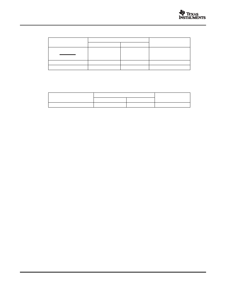
Table 4. Test-Mode-Select Address
VALUE SHIFTED INTO DATA INPUT
INTERNAL SELF-TEST
UNIPOLAR OUTPUT
VOLTAGE SELECTED(1)
RESULT (HEX)(2)
BINARY
HEX
1011
B
800
Vref–
1100
C
000
Vref+
1101
D
FFF
(1)
Vref+ is the voltage applied to REF+, and Vref– is the voltage applied to REF–.
(2)
The output results shown are the ideal values and may vary with the reference stability and with
internal offsets.
Table 5. Power-Down-Select Address
VALUE SHIFTED INTO DATA INPUT
INPUT COMMAND
RESULT
BINARY
HEX
Power down
1110
E
ICC ≤25 A
The CMOS threshold detector in the successive-approximation conversion system determines each bit by
examining the charge on a series of binary-weighted capacitors (see Figure 1). In the first phase of the
conversion process, the analog input is sampled by closing the SC switch and all ST switches simultaneously.
This action charges all the capacitors to the input voltage.
In the next phase of the conversion process, all ST and SC switches are opened and the threshold detector
begins identifying bits by identifying the charge (voltage) on each capacitor relative to the reference (REF–)
voltage. In the switching sequence, 12 capacitors are examined separately until all 12 bits are identified and the
charge-convert sequence is repeated. In the first step of the conversion phase, the threshold detector looks at
the first capacitor (weight = 4096). Node 4096 of this capacitor is switched to the REF+ voltage, and the
equivalent nodes of all the other capacitors on the ladder are switched to REF–. When the voltage at the
summing node is greater than the trip point of the threshold detector (approximately one-half VCC), a bit 0 is
placed in the output register and the 4096-weight capacitor is switched to REF–. When the voltage at the
summing node is less than the trip point of the threshold detector, a bit 1 is placed in the register and this
4096-weight capacitor remains connected to REF+ through the remainder of the successive-approximation
process. The process is repeated for the 2048-weight capacitor, the 1024-weight capacitor, and so forth down
the line until all bits are determined. With each step of the successive-approximation process, the initial charge
is redistributed among the capacitors. The conversion process relies on charge redistribution to determine the
bits from MSB to LSB.
The two reference inputs used with the device are the voltages applied to the REF+ and REF– terminals. These
voltage values establish the upper and lower limits of the analog input to produce a full-scale and zero-scale
reading, respectively. These voltages and the analog input should not exceed the positive supply or be lower
than ground consistent with the specified absolute maximum ratings. The digital output is at full scale when the
input signal is equal to or higher than REF+ terminal voltage, and at zero when the input signal is equal to or
lower than REF– terminal voltage.
18
相关PDF资料 |
PDF描述 |
|---|---|
| TLC2543MFK | 11-CH 12-BIT SUCCESSIVE APPROXIMATION ADC, SERIAL ACCESS, CQCC20 |
| TLC2552IDGK | 2-CH 12-BIT SUCCESSIVE APPROXIMATION ADC, SERIAL ACCESS, PDSO8 |
| TLC2552IDR | 2-CH 12-BIT SUCCESSIVE APPROXIMATION ADC, SERIAL ACCESS, PDSO8 |
| TLC2555IDGK | 1-CH 12-BIT SUCCESSIVE APPROXIMATION ADC, SERIAL ACCESS, PDSO8 |
| TLC2555IDR | 1-CH 12-BIT SUCCESSIVE APPROXIMATION ADC, SERIAL ACCESS, PDSO8 |
相关代理商/技术参数 |
参数描述 |
|---|---|
| TLC254ACD | 功能描述:运算放大器 - 运放 Quad LinCMOS RoHS:否 制造商:STMicroelectronics 通道数量:4 共模抑制比(最小值):63 dB 输入补偿电压:1 mV 输入偏流(最大值):10 pA 工作电源电压:2.7 V to 5.5 V 安装风格:SMD/SMT 封装 / 箱体:QFN-16 转换速度:0.89 V/us 关闭:No 输出电流:55 mA 最大工作温度:+ 125 C 封装:Reel |
| TLC254ACDG4 | 功能描述:运算放大器 - 运放 LinCMOS Quad OP AMP RoHS:否 制造商:STMicroelectronics 通道数量:4 共模抑制比(最小值):63 dB 输入补偿电压:1 mV 输入偏流(最大值):10 pA 工作电源电压:2.7 V to 5.5 V 安装风格:SMD/SMT 封装 / 箱体:QFN-16 转换速度:0.89 V/us 关闭:No 输出电流:55 mA 最大工作温度:+ 125 C 封装:Reel |
| TLC254ACN | 功能描述:运算放大器 - 运放 Lin CMOS Quad RoHS:否 制造商:STMicroelectronics 通道数量:4 共模抑制比(最小值):63 dB 输入补偿电压:1 mV 输入偏流(最大值):10 pA 工作电源电压:2.7 V to 5.5 V 安装风格:SMD/SMT 封装 / 箱体:QFN-16 转换速度:0.89 V/us 关闭:No 输出电流:55 mA 最大工作温度:+ 125 C 封装:Reel |
| TLC254ACNE4 | 功能描述:运算放大器 - 运放 LinCMOS Quad Op Amp RoHS:否 制造商:STMicroelectronics 通道数量:4 共模抑制比(最小值):63 dB 输入补偿电压:1 mV 输入偏流(最大值):10 pA 工作电源电压:2.7 V to 5.5 V 安装风格:SMD/SMT 封装 / 箱体:QFN-16 转换速度:0.89 V/us 关闭:No 输出电流:55 mA 最大工作温度:+ 125 C 封装:Reel |
| TLC254BCD | 功能描述:运算放大器 - 运放 LinCMOS Quad RoHS:否 制造商:STMicroelectronics 通道数量:4 共模抑制比(最小值):63 dB 输入补偿电压:1 mV 输入偏流(最大值):10 pA 工作电源电压:2.7 V to 5.5 V 安装风格:SMD/SMT 封装 / 箱体:QFN-16 转换速度:0.89 V/us 关闭:No 输出电流:55 mA 最大工作温度:+ 125 C 封装:Reel |
发布紧急采购,3分钟左右您将得到回复。