- 您现在的位置:买卖IC网 > PDF目录98236 > TLC2558CPWR (TEXAS INSTRUMENTS INC) 8-CH 12-BIT SUCCESSIVE APPROXIMATION ADC, SERIAL ACCESS, PDSO20 PDF资料下载
参数资料
| 型号: | TLC2558CPWR |
| 厂商: | TEXAS INSTRUMENTS INC |
| 元件分类: | ADC |
| 英文描述: | 8-CH 12-BIT SUCCESSIVE APPROXIMATION ADC, SERIAL ACCESS, PDSO20 |
| 封装: | GREEN, PLASTIC, TSSOP-20 |
| 文件页数: | 11/48页 |
| 文件大小: | 1074K |
| 代理商: | TLC2558CPWR |
第1页第2页第3页第4页第5页第6页第7页第8页第9页第10页当前第11页第12页第13页第14页第15页第16页第17页第18页第19页第20页第21页第22页第23页第24页第25页第26页第27页第28页第29页第30页第31页第32页第33页第34页第35页第36页第37页第38页第39页第40页第41页第42页第43页第44页第45页第46页第47页第48页
TLC2554, TLC2558
5-V, 12-BIT, 400 KSPS, 4/8 CHANNEL, LOW POWER,
SERIAL ANALOG-TO-DIGITAL CONVERTERS WITH AUTO POWER DOWN
SLAS220A –JUNE 1999
19
POST OFFICE BOX 655303
DALLAS, TEXAS 75265
FIFO operation (continued)
power down
Writing 8000h to the device puts the device into a software power-down state. For a hardware power down, the
dedicated PWDN pin provides another way to power down the device asynchronously. These two power-down
modes power down the entire device including the built-in reference to save power. It requires 20 ms to resume
from either a software or hardware power down.
Auto power down mode is always enabled. This mode maintains the built-in reference if an internal reference
is used, so resumption is fast enough to be used between cycles.
The configuration register is not affected by any of the power down modes but the sweep operation sequence
has to be started over again. All FIFO contents are cleared by the power-down modes.
power up and initialization
Initialization requires:
1.
Determine processor type by writing A000h to the TLC2554/58
2.
Configure the device
The first conversion after power up or resuming from power down is not valid.
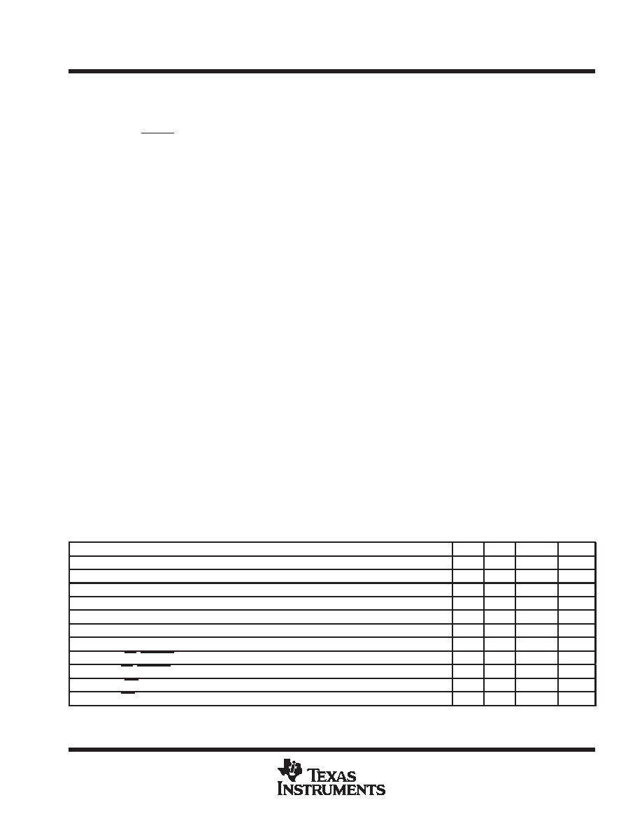
absolute maximum ratings over operating free-air temperature (unless otherwise noted)
Supply voltage range, GND to VCC
–0.3 V to 6.5 V
. . . . . . . . . . . . . . . . . . . . . . . . . . . . . . . . . . . . . . . . . . . . . . . . .
Analog input voltage range
–0.3 V to VCC + 0.3 V
. . . . . . . . . . . . . . . . . . . . . . . . . . . . . . . . . . . . . . . . . . . . . . . . . . .
Reference input voltage
VCC + 0.3 V
. . . . . . . . . . . . . . . . . . . . . . . . . . . . . . . . . . . . . . . . . . . . . . . . . . . . . . . . . . . . .
Digital input voltage range
–0.3 V to VCC + 0.3 V
. . . . . . . . . . . . . . . . . . . . . . . . . . . . . . . . . . . . . . . . . . . . . . . . . . .
Operating virtual junction temperature range, TJ
–40
°C to 150°C
. . . . . . . . . . . . . . . . . . . . . . . . . . . . . . . . . . . . .
Operating free-air temperature range, TA: TLC2554/58C
0
°C to 70°C
. . . . . . . . . . . . . . . . . . . . . . . . . . . . . . . .
TLC2554/58I
–40
°C to 85°C
. . . . . . . . . . . . . . . . . . . . . . . . . . . . . . .
Storage temperature range, Tstg
–65
°C to 150°C
. . . . . . . . . . . . . . . . . . . . . . . . . . . . . . . . . . . . . . . . . . . . . . . . . . .
Lead temperature 1,6 mm (1/16 inch) from case for 10 seconds
260
°C
. . . . . . . . . . . . . . . . . . . . . . . . . . . . . . .
Stresses beyond those listed under “absolute maximum ratings” may cause permanent damage to the device. These are stress ratings only, and
functional operation of the device at these or any other conditions beyond those indicated under “recommended operating conditions” is not
implied. Exposure to absolute-maximum-rated conditions for extended periods may affect device reliability.
recommended operating conditions
MIN
NOM
MAX
UNIT
Supply voltage, VCC
4.5
5
5.5
V
Positive external reference voltage input, VREFP (see Note 1)
2
VCC
V
Negative external reference voltage input, VREFM (note Note 1)
0
2
V
Differential reference voltage input, VREFP – VREFM (see Note 1)
2
VCC VCC+0.2
V
Analog input voltage (see Note 1)
0
VCC
V
High level control input voltage, VIH
2.1
V
Low-level control input voltage, VIL
0.6
V
Rise time, for CS, CSTART SDI at 0.5 pF, tr(I/O)
4.76
ns
Fall time, for CS, CSTART SDI at 0.5 pF, tf(I/O)
2.91
ns
Rise time, for INT, EOC, SDO at 30 pF, tr(Output)
2.43
ns
Fall time, for INT, EOC, SDO at 30 pF, tf(Output)
2.3
ns
NOTE 1: When binary output format is used, analog input voltages greater than that applied to REFP convert as all ones (111111111111), while
input voltages less than that applied to REFM convert as all zeros (000000000000). The device is functional with reference down to
2 V (VREFP – VREFM –1); however, the electrical specifications are no longer applicable.
相关PDF资料 |
PDF描述 |
|---|---|
| TLC2558CPWRG4 | 8-CH 12-BIT SUCCESSIVE APPROXIMATION ADC, SERIAL ACCESS, PDSO20 |
| TLC2554ID | 4-CH 12-BIT SUCCESSIVE APPROXIMATION ADC, SERIAL ACCESS, PDSO16 |
| TLC2554IDR | 4-CH 12-BIT SUCCESSIVE APPROXIMATION ADC, SERIAL ACCESS, PDSO16 |
| TLC2554QDR | 4-CH 12-BIT SUCCESSIVE APPROXIMATION ADC, SERIAL ACCESS, PDSO16 |
| TLC2554QD | 4-CH 12-BIT SUCCESSIVE APPROXIMATION ADC, SERIAL ACCESS, PDSO16 |
相关代理商/技术参数 |
参数描述 |
|---|---|
| TLC2558CPWRG4 | 功能描述:模数转换器 - ADC 12-bit 400 KSPS 8-Ch Serial w/Powerdown RoHS:否 制造商:Texas Instruments 通道数量:2 结构:Sigma-Delta 转换速率:125 SPs to 8 KSPs 分辨率:24 bit 输入类型:Differential 信噪比:107 dB 接口类型:SPI 工作电源电压:1.7 V to 3.6 V, 2.7 V to 5.25 V 最大工作温度:+ 85 C 安装风格:SMD/SMT 封装 / 箱体:VQFN-32 |
| TLC2558IDW | 功能描述:模数转换器 - ADC 12bit3 200kSPS SAR RoHS:否 制造商:Texas Instruments 通道数量:2 结构:Sigma-Delta 转换速率:125 SPs to 8 KSPs 分辨率:24 bit 输入类型:Differential 信噪比:107 dB 接口类型:SPI 工作电源电压:1.7 V to 3.6 V, 2.7 V to 5.25 V 最大工作温度:+ 85 C 安装风格:SMD/SMT 封装 / 箱体:VQFN-32 |
| TLC2558IDWG4 | 功能描述:模数转换器 - ADC 12bit3 200kSPS SAR RoHS:否 制造商:Texas Instruments 通道数量:2 结构:Sigma-Delta 转换速率:125 SPs to 8 KSPs 分辨率:24 bit 输入类型:Differential 信噪比:107 dB 接口类型:SPI 工作电源电压:1.7 V to 3.6 V, 2.7 V to 5.25 V 最大工作温度:+ 85 C 安装风格:SMD/SMT 封装 / 箱体:VQFN-32 |
| TLC2558IDWR | 功能描述:模数转换器 - ADC 12-bit 400 KSPS 8-Ch Serial w/Powerdown RoHS:否 制造商:Texas Instruments 通道数量:2 结构:Sigma-Delta 转换速率:125 SPs to 8 KSPs 分辨率:24 bit 输入类型:Differential 信噪比:107 dB 接口类型:SPI 工作电源电压:1.7 V to 3.6 V, 2.7 V to 5.25 V 最大工作温度:+ 85 C 安装风格:SMD/SMT 封装 / 箱体:VQFN-32 |
| TLC2558IDWRG4 | 功能描述:模数转换器 - ADC 12-bit 400 KSPS 8-Ch Serial w/Powerdown RoHS:否 制造商:Texas Instruments 通道数量:2 结构:Sigma-Delta 转换速率:125 SPs to 8 KSPs 分辨率:24 bit 输入类型:Differential 信噪比:107 dB 接口类型:SPI 工作电源电压:1.7 V to 3.6 V, 2.7 V to 5.25 V 最大工作温度:+ 85 C 安装风格:SMD/SMT 封装 / 箱体:VQFN-32 |
发布紧急采购,3分钟左右您将得到回复。