- 您现在的位置:买卖IC网 > PDF目录382605 > TLC2652A-8D (Texas Instruments, Inc.) CONNECTOR ACCESSORY PDF资料下载
参数资料
| 型号: | TLC2652A-8D |
| 厂商: | Texas Instruments, Inc. |
| 英文描述: | CONNECTOR ACCESSORY |
| 中文描述: | 连接器附件 |
| 文件页数: | 22/31页 |
| 文件大小: | 474K |
| 代理商: | TLC2652A-8D |
第1页第2页第3页第4页第5页第6页第7页第8页第9页第10页第11页第12页第13页第14页第15页第16页第17页第18页第19页第20页第21页当前第22页第23页第24页第25页第26页第27页第28页第29页第30页第31页
TLC2652, TLC2652A, TLC2652Y
Advanced LinCMOS
PRECISION CHOPPER-STABILIZED
OPERATIONAL AMPLIFIERS
SLOS019C – SEPTEMBER 1988 – REVISED FEBRUARY 1999
22
POST OFFICE BOX 655303
DALLAS, TEXAS 75265
APPLICATION INFORMATION
internal/external clock
The TLC2652 has an internal clock that sets the chopping frequency to a nominal value of 450 Hz. On 8-pin
packages, the chopping frequency can only be controlled by the internal clock; however, on all 14-pin packages
and the 20-pin FK package, the device chopping frequency can be set by the internal clock or controlled
externally by use of the INT/EXT and CLK IN pins. To use the internal 450-Hz clock, no connection is necessary.
If external clocking is desired, connect INT/EXT to V
DD–
and the external clock to CLK IN. The external clock
trip point is 2.5 V above the negative rail; however, CLK IN can be driven from the negative rail to 5 V above
the negative rail. If this level is exceeded, damage could occur to the device unless the current into CLK IN is
limited to
±
5 mA. When operating in the single-supply configuration, this feature allows the TLC2652 to be driven
directly by 5-V TTL and CMOS logic. A
divide-by-two frequency divider interfaces with
CLK IN and sets the clock chopping frequency.
The duty cycle of the external is not critical but
should be kept between 30% and 60%.
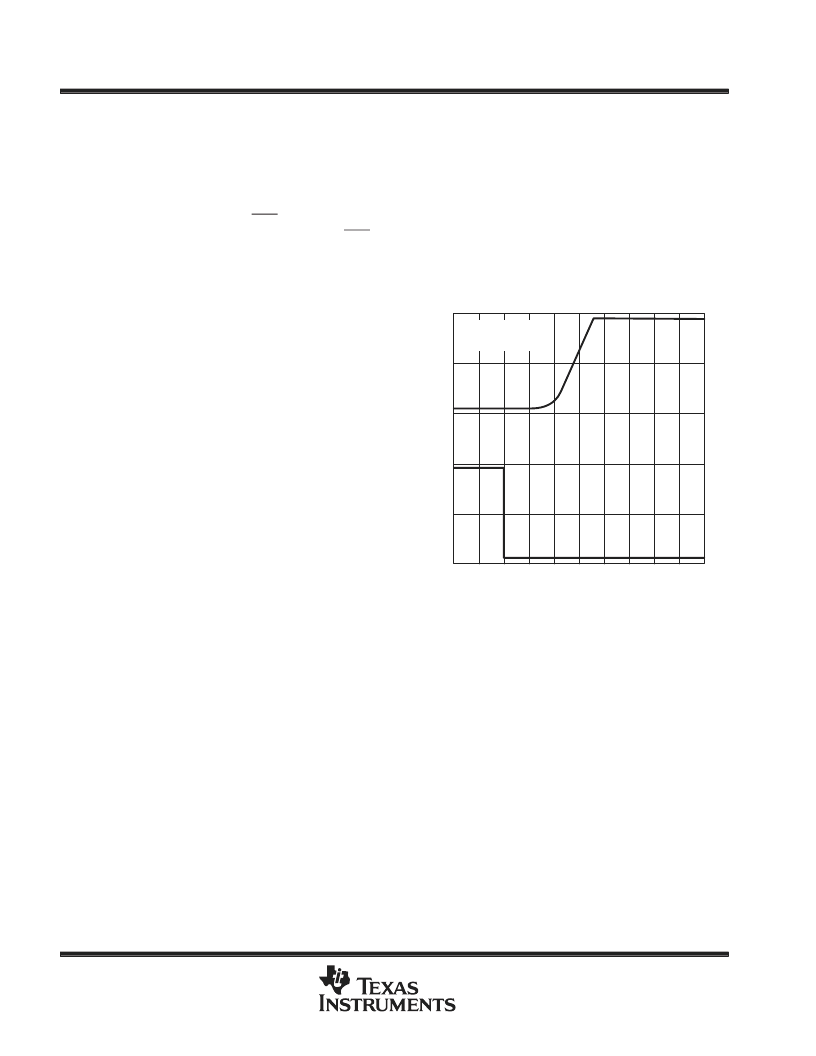
overload recovery/output clamp
When large differential input voltage conditions
are applied to the TLC2652, the nulling loop
attempts to prevent the output from saturating by
driving C
XA
and C
XB
to internally-clamped voltage
levels. Once the overdrive condition is removed,
a period of time is required to allow the built-up
charge to dissipate. This time period is defined as
overload recovery time (see Figure 33). Typical
overload recovery time for the TLC2652 is
significantly faster than competitive products;
however, if required, this time can be reduced
further by use of internal clamp circuitry
accessible through CLAMP if required.
The clamp is a switch that is automatically activated when the output is approximately 1 V from either supply
rail. When connected to the inverting input (in parallel with the closed-loop feedback resistor), the closed-loop
gain is reduced, and the TLC2652 output is prevented from going into saturation. Since the output must source
sink current through the switch (see Figure 7), the maximum output voltage swing is slightly reduced.
thermoelectric effects
To take advantage of the extremely low offset voltage drift of the TLC2652, care must be taken to compensate
for the thermoelectric effects present when two dissimilar metals are brought into contact with each other (such
as device leads being soldered to a printed circuit board). Dissimilar metal junctions can produce thermoelectric
voltages in the range of several microvolts per degree Celsius (orders of magnitude greater than the 0.01-
μ
V/
°
C
typical of the TLC2652).
To help minimize thermoelectric effects, careful attention should be paid to component selection and
circuit-board layout. Avoid the use of nonsoldered connections (such as sockets, relays, switches, etc.) in the
input signal path. Cancel thermoelectric effects by duplicating the number of components and junctions in each
device input. The use of low-thermoelectric-coefficient components, such as wire-wound resistors, is also
beneficial.
0
0
10
20
t – Time – ms
30
40
V
0
50
60
70
80
V
VDD
±
=
±
5 V
TA = 25
°
C
Figure 33. Overload Recovery
–5
–50
相关PDF资料 |
PDF描述 |
|---|---|
| TLC2652AMFK | Advanced LinCMOSE PRECISION CHOPPER-STABILIZED OPERATIONAL AMPLIFIERS |
| TLC2652AMJ | Advanced LinCMOSE PRECISION CHOPPER-STABILIZED OPERATIONAL AMPLIFIERS |
| TLC2652AMN | Advanced LinCMOSE PRECISION CHOPPER-STABILIZED OPERATIONAL AMPLIFIERS |
| TLC2652AMP | Advanced LinCMOSE PRECISION CHOPPER-STABILIZED OPERATIONAL AMPLIFIERS |
| TLC2652IN | Advanced LinCMOSE PRECISION CHOPPER-STABILIZED OPERATIONAL AMPLIFIERS |
相关代理商/技术参数 |
参数描述 |
|---|---|
| TLC2652AC-14D | 功能描述:运算放大器 - 运放 Adv Prec. Chopper RoHS:否 制造商:STMicroelectronics 通道数量:4 共模抑制比(最小值):63 dB 输入补偿电压:1 mV 输入偏流(最大值):10 pA 工作电源电压:2.7 V to 5.5 V 安装风格:SMD/SMT 封装 / 箱体:QFN-16 转换速度:0.89 V/us 关闭:No 输出电流:55 mA 最大工作温度:+ 125 C 封装:Reel |
| TLC2652AC-14DG4 | 功能描述:运算放大器 - 运放 LinCMOS Chopper Stabilized OP AMP RoHS:否 制造商:STMicroelectronics 通道数量:4 共模抑制比(最小值):63 dB 输入补偿电压:1 mV 输入偏流(最大值):10 pA 工作电源电压:2.7 V to 5.5 V 安装风格:SMD/SMT 封装 / 箱体:QFN-16 转换速度:0.89 V/us 关闭:No 输出电流:55 mA 最大工作温度:+ 125 C 封装:Reel |
| TLC2652AC-8D | 功能描述:运算放大器 - 运放 Adv Prec. Chopper RoHS:否 制造商:STMicroelectronics 通道数量:4 共模抑制比(最小值):63 dB 输入补偿电压:1 mV 输入偏流(最大值):10 pA 工作电源电压:2.7 V to 5.5 V 安装风格:SMD/SMT 封装 / 箱体:QFN-16 转换速度:0.89 V/us 关闭:No 输出电流:55 mA 最大工作温度:+ 125 C 封装:Reel |
| TLC2652AC-8DG4 | 功能描述:运算放大器 - 运放 Adv LinCMOS Prec Chopper-Stabilized RoHS:否 制造商:STMicroelectronics 通道数量:4 共模抑制比(最小值):63 dB 输入补偿电压:1 mV 输入偏流(最大值):10 pA 工作电源电压:2.7 V to 5.5 V 安装风格:SMD/SMT 封装 / 箱体:QFN-16 转换速度:0.89 V/us 关闭:No 输出电流:55 mA 最大工作温度:+ 125 C 封装:Reel |
| TLC2652ACN | 功能描述:运算放大器 - 运放 Adv Prec. Chopper RoHS:否 制造商:STMicroelectronics 通道数量:4 共模抑制比(最小值):63 dB 输入补偿电压:1 mV 输入偏流(最大值):10 pA 工作电源电压:2.7 V to 5.5 V 安装风格:SMD/SMT 封装 / 箱体:QFN-16 转换速度:0.89 V/us 关闭:No 输出电流:55 mA 最大工作温度:+ 125 C 封装:Reel |
发布紧急采购,3分钟左右您将得到回复。