- 您现在的位置:买卖IC网 > PDF目录97203 > TLC2934IPW (TEXAS INSTRUMENTS INC) PHASE LOCKED LOOP, 130 MHz, PDSO14 PDF资料下载
参数资料
| 型号: | TLC2934IPW |
| 厂商: | TEXAS INSTRUMENTS INC |
| 元件分类: | PLL合成/DDS/VCOs |
| 英文描述: | PHASE LOCKED LOOP, 130 MHz, PDSO14 |
| 封装: | GREEN, PLASTIC, TSSOP-14 |
| 文件页数: | 3/10页 |
| 文件大小: | 272K |
| 代理商: | TLC2934IPW |
TLC2934
3.3 V 130 MHZ VCO, PHASE FREQUENCY DETECTOR
SLAS306 – NOVEMBER 2000
2
POST OFFICE BOX 655303
DALLAS, TEXAS 75265
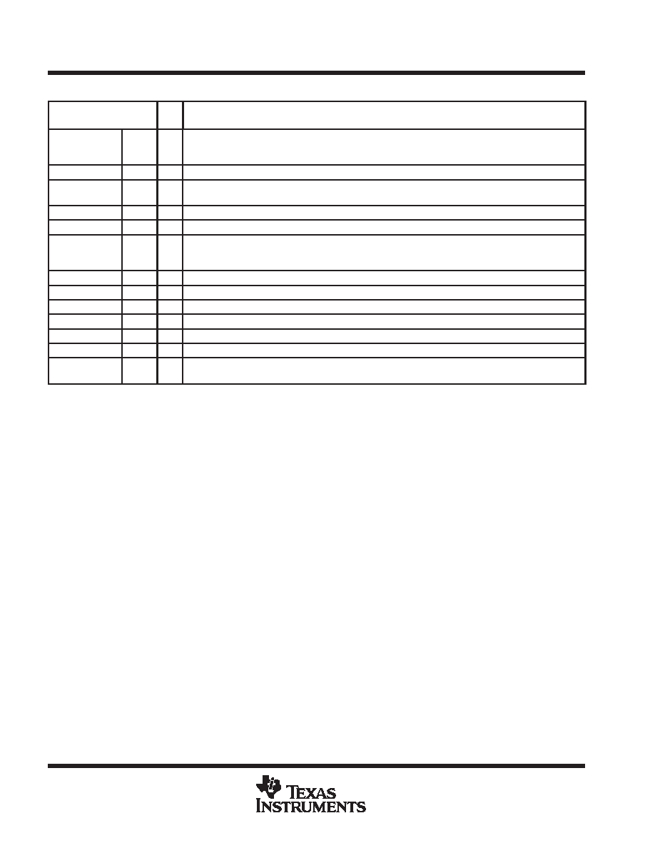
Terminal Functions
TERMINAL
I/O
DESCRIPTION
NAME
NO.
I/O
DESCRIPTION
FIN-A,
FIN-B
4
5
I
Frequency signal inputs for PFD. The reference frequency signal (fREF-IN) and the VCO output signal
through the external counter device are applied to these terminals. When the LPF design is the lag-lead filter
(passive filter and noninverting), f(REF-IN) is input to FIN-A, and the VCO output signal is to FIN-B.
LOGIC GND
7
GND terminal for the internal logic circuit
LOGIC VDD
1
Power supply terminal for the internal logic circuit. This power supply terminal separates from VCO VDD to
reduce cross-coupling between supplies.
PFD INHIBIT
9
I
PFD INHIBIT (power-down) control signal input terminal
PFD OUT
6
O
PFD output terminal. When PFD INHIBIT is high, PFD OUT is in the high-impedance state.
RBIAS
13
I
Bias resistor (RBIAS) terminal. Connect a resistor between VCO GND and this terminal to supply bias to
internal VCO circuit. TLC2934 bias resistor connection is different from TLC2932 and TLC2933, where bias
resistor RBIAS is connected to VCO VDD.
SELECT
2
I
1/2 divider select terminal. L=through output, H=1/2 output.
TEST
8
Test terminal. Use for production test. Tie to GND when in normal use.
VCO GND
11
GND terminal for internal VCO
VCO OUT
3
O
VCO output terminal. When VCO INHIBIT = high, VCO OUT is low.
VCO INHIBIT
10
I
VCO INHIBIT (power-down) control signal input terminal
VCO IN
12
I
VCO control voltage input terminal. Normally, The external LPF is connected to this terminal.
VCO VDD
14
Power supply terminal for the internal VCO circuit. This power supply terminal should be separate from
LOGIC VDD to reduce cross-coupling between supplies.
absolute maximum ratings over operating free-air temperature (unless otherwise noted)
Supply voltage (each supply), VDD (see Note 1)
–0.5 V to 4 V
. . . . . . . . . . . . . . . . . . . . . . . . . . . . . . . . . . . . . . .
Input voltage range (each input), VI (see Note 1)
–0.5 V to VDD + 0.5 V
. . . . . . . . . . . . . . . . . . . . . . . . . . . . . . . .
Input current (each input), II
±20 mA
. . . . . . . . . . . . . . . . . . . . . . . . . . . . . . . . . . . . . . . . . . . . . . . . . . . . . . . . . . . . . .
Output current (each output), IO
±20 mA
. . . . . . . . . . . . . . . . . . . . . . . . . . . . . . . . . . . . . . . . . . . . . . . . . . . . . . . . . .
Continuous total power dissipation at (or below) TA = 25_C (see Note 2), PD
700 mW
. . . . . . . . . . . . . . . . . . .
Operating free-air temperature range. TA
–20
°C to 75°C
. . . . . . . . . . . . . . . . . . . . . . . . . . . . . . . . . . . . . . . . . . .
Storage temperature range, Tstg
–65
°C to 150°C
. . . . . . . . . . . . . . . . . . . . . . . . . . . . . . . . . . . . . . . . . . . . . . . . . . .
Lead temperature 1,6 mm (1/16 inch) from case for 10 seconds
260
°C
. . . . . . . . . . . . . . . . . . . . . . . . . . . . . . .
Stresses beyond those listed under “absolute maximum ratings” may cause permanent damage to the device. These are stress ratings only, and
functional operation of the device at these or any other conditions beyond those indicated under “recommended operating conditions” is not
implied. Exposure to absolute-maximum-rated conditions for extended periods may affect device reliability.
NOTES:
1. All voltage values are with respect to network ground terminal.
2. For operation above 25
°C free–air temperature, derate linearly at the rate of 5.6 mW/°C
相关PDF资料 |
PDF描述 |
|---|---|
| TLC4016MN | QUAD 1-CHANNEL, SGL POLE SGL THROW SWITCH, PDIP14 |
| TLC532AIFN | 8-BIT SUCCESSIVE APPROXIMATION ADC, PARALLEL ACCESS, PQCC28 |
| TLC532AIN | 8-BIT SUCCESSIVE APPROXIMATION ADC, PARALLEL ACCESS, PDIP28 |
| TLC533AIFN | 8-BIT SUCCESSIVE APPROXIMATION ADC, PARALLEL ACCESS, PQCC28 |
| TLC533AMFN | 8-BIT SUCCESSIVE APPROXIMATION ADC, PARALLEL ACCESS, PQCC28 |
相关代理商/技术参数 |
参数描述 |
|---|---|
| TLC2934IPWG4 | 功能描述:相位探测器 / 移相器 High Perform Sngl Locked Loop RoHS:否 制造商:M/A-COM Technology Solutions 封装 / 箱体:PQFN-24 封装:Reel |
| TLC2934IPWR | 功能描述:相位探测器 / 移相器 Hi Perf Sngl Phase Locked Loop RoHS:否 制造商:M/A-COM Technology Solutions 封装 / 箱体:PQFN-24 封装:Reel |
| TLC2934IPWRG4 | 功能描述:IC PHASE LOCK LOOP HP 14-TSSOP RoHS:是 类别:集成电路 (IC) >> 时钟/计时 - 时钟发生器,PLL,频率合成器 系列:- 标准包装:27 系列:Precision Edge® 类型:频率合成器 PLL:是 输入:PECL,晶体 输出:PECL 电路数:1 比率 - 输入:输出:1:1 差分 - 输入:输出:无/是 频率 - 最大:800MHz 除法器/乘法器:是/无 电源电压:3.135 V ~ 5.25 V 工作温度:0°C ~ 85°C 安装类型:表面贴装 封装/外壳:28-SOIC(0.295",7.50mm 宽) 供应商设备封装:28-SOIC 包装:管件 |
| TLC2940IPW | 制造商:Rochester Electronics LLC 功能描述:- Bulk 制造商:Texas Instruments 功能描述: |
| TLC2942IDB | 制造商:Rochester Electronics LLC 功能描述:- Bulk |
发布紧急采购,3分钟左右您将得到回复。