- 您现在的位置:买卖IC网 > PDF目录382606 > TLC320A545I (Texas Instruments, Inc.) SMA (F) TO MCX (M) ADAPTERS PDF资料下载
参数资料
| 型号: | TLC320A545I |
| 厂商: | Texas Instruments, Inc. |
| 英文描述: | SMA (F) TO MCX (M) ADAPTERS |
| 中文描述: | 单信道数据/传真编解码器 |
| 文件页数: | 17/35页 |
| 文件大小: | 174K |
| 代理商: | TLC320A545I |
第1页第2页第3页第4页第5页第6页第7页第8页第9页第10页第11页第12页第13页第14页第15页第16页当前第17页第18页第19页第20页第21页第22页第23页第24页第25页第26页第27页第28页第29页第30页第31页第32页第33页第34页第35页
4–1
4 Serial Communications
DT_DOUT, DT_DIN, DT_SCLK, and DT_FS, are the serial communication signals for the serial port. The digital
output data from the ADC is taken from DT_DOUT. The digital input data for the DAC is applied to DT_DIN. The
synchronization clock for the serial communication data and the frame-sync is taken from DT_SCLK. The frame-sync
pulse, which signals the beginning of the ADC and DAC data transfer interval, is taken from DT_FS.
For signal data transmitted from the ADC or to the DAC, a primary serial communication is used. A secondary
communication is used to read or write words to the control registers, which control both the options and the circuit
configurations of the device.
The purpose of the primary and secondary communications is to allow conversion data and control data to be
transferred across the same serial port. A primary transfer is always dedicated to conversion data. A secondary
transfer is used to set up or read the control register values described in Appendix A Programmable Register Set.
A primary transfer occurs for every conversion period. A secondary transfer occurs only when requested. Secondary
serial communication is requested by software (D0 of the primary data input to DT_DIN). Control registers 1 and 2
can only be read/write from/to the serial port.
4.1
Primary Serial Communication
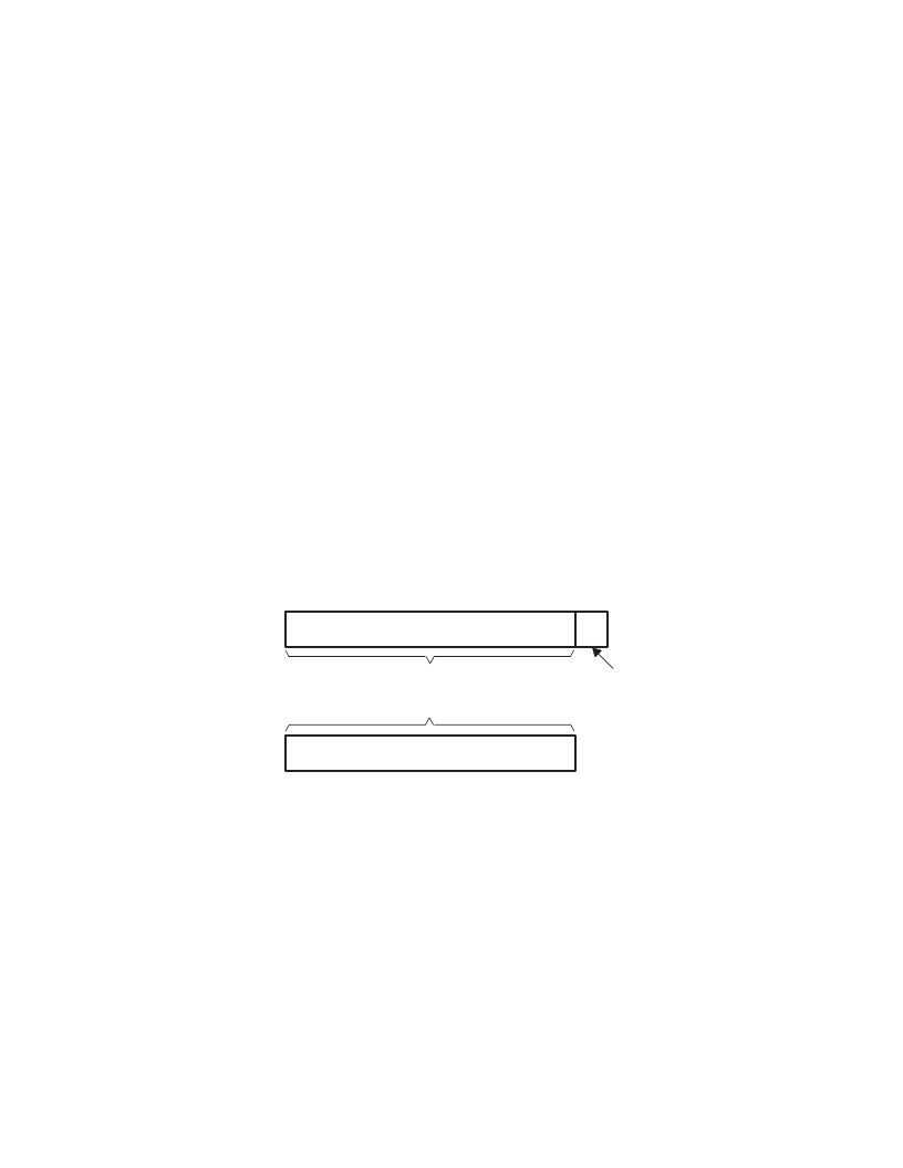
Primary serial communication is used to both transmit and receive conversion signal data. The DAC word length is
15 bits and the last bit of the primary 16-bit serial communication word is a control bit used to request secondary serial
communication. For all serial communications, the most significant bit is transferred first. For the 16-bit ADC word,
D15 is the most significant bit and D0 is the least significant bit. For the 15-bit DAC data word in a primary
communication, D15 is the most significant bit, D1 is the least significant bit, and D0 is used for the secondary
communication request control. All digital data values are in 2s-complement data format. Refer to Figure 4–1.
D15–D1
D0
DT_DIN
D15–D0
A/D Data
DT_DOUT
Secondary
Communication Request
D/A Data
Figure 4–1. Primary Communication DIN and DOUT Data Format
相关PDF资料 |
PDF描述 |
|---|---|
| TLC339QD | DIODE ZENER DUAL ISOLATED 200mW 24Vz 5.2mA-Izt 0.05 0.1uA-Ir 18 SOT-363 3K/REEL |
| TLC139D | LinCMOSE MICROPOWER QUAD COMPARATORS |
| TLC139FK | LinCMOSE MICROPOWER QUAD COMPARATORS |
| TLC139J | MOSFET N-CH 400V 3.1A I-PAK |
| TLC139MFK | LinCMOSE MICROPOWER QUAD COMPARATORS |
相关代理商/技术参数 |
参数描述 |
|---|---|
| TLC320AC01 | 制造商:TI 制造商全称:Texas Instruments 功能描述:Single-Supply Analog Interface Circuit |
| TLC320AC01C | 制造商:TI 制造商全称:Texas Instruments 功能描述:Single-Supply Analog Interface Circuit |
| TLC320AC01CFN | 功能描述:接口—CODEC SNGL CH Codec Bandwidth Indpendent RoHS:否 制造商:Texas Instruments 类型: 分辨率: 转换速率:48 kSPs 接口类型:I2C ADC 数量:2 DAC 数量:4 工作电源电压:1.8 V, 2.1 V, 2.3 V to 5.5 V 最大工作温度:+ 85 C 安装风格:SMD/SMT 封装 / 箱体:DSBGA-81 封装:Reel |
| TLC320AC01CFN | 制造商:Texas Instruments 功能描述:Special Function IC Package/Case:20-PLCC |
| TLC320AC01CFNR | 功能描述:接口—CODEC SNGL CH Codec Bandwidth Indpendent RoHS:否 制造商:Texas Instruments 类型: 分辨率: 转换速率:48 kSPs 接口类型:I2C ADC 数量:2 DAC 数量:4 工作电源电压:1.8 V, 2.1 V, 2.3 V to 5.5 V 最大工作温度:+ 85 C 安装风格:SMD/SMT 封装 / 箱体:DSBGA-81 封装:Reel |
发布紧急采购,3分钟左右您将得到回复。