- 您现在的位置:买卖IC网 > PDF目录382606 > TLC3545IDGKR (Texas Instruments, Inc.) 5-V. LOW POWER, 14-BIT, 200-KSPS SERIAL ANALOG-TO-DIGITAL CONVERTERS WITH AUTO-POWER DOWN PDF资料下载
参数资料
| 型号: | TLC3545IDGKR |
| 厂商: | Texas Instruments, Inc. |
| 英文描述: | 5-V. LOW POWER, 14-BIT, 200-KSPS SERIAL ANALOG-TO-DIGITAL CONVERTERS WITH AUTO-POWER DOWN |
| 中文描述: | 5 - V等。低功耗,14位200 ksps的串行模数位自动转换器掉电 |
| 文件页数: | 13/23页 |
| 文件大小: | 481K |
| 代理商: | TLC3545IDGKR |
SLAS345 DECEMBER 2001
13
www.ti.com
PRINCIPLES OF OPERATION
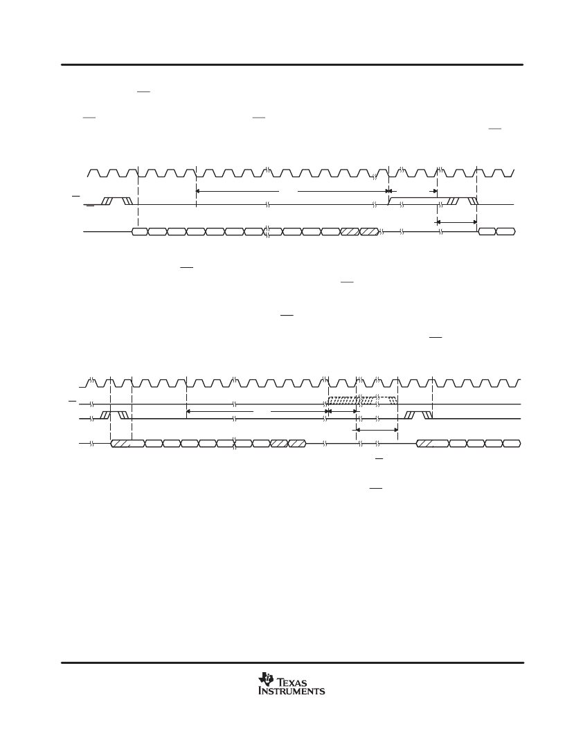
control via pin 1 (CS, DSP interface)
All devices are compatible with this mode of operation. The FS signal from a DSP is connected directly to the
CS input of the ADC.
A falling edge on the CS input while SCLK is high or low initiates the cycle.
(For TLC3541
in this configuration, the FS input is tied to V
DD
.)
Enough time should be allowed before the next rising CS edge
so that the conversion cycle is not terminated prematurely.
1
2
3
5
4
6
7
13
14
15
16
1
12
ts
tconv
t(PWRDWN)
SDO Data Is the Result of the Previous Sample
For TLC35xx, the LSB Is Presented on the Rising SCLK 14th Edge
MSB
MSB1
MSB2
MSB3 MSB4 MSB5 MSB6
LSB+2
LSB+1
LSB
LSB1
LSB2
SCLK
CS
SDO
MSB
MSB1
The CS Input Signal Is
Generated by the FS Output
From a TMS320 DSP
24
Figure 16. DSP Cycle Timing Using the CS Input (FS = 1 for TLC3541 only)
control via pin 1 and pin 7 (CS and FS or FS only, DSP interface)
Only TLC3541 is compatible with this mode of operation. The CS input to the ADC can be controlled via a
general-purpose I/O pin from the DSP or tied to ground. The FS signal from the DSP is connected directly to
the FS input of the ADC. A rising FS edge releases the MSB to the SDO output. The falling edge on the FS input
while SCLK is high or low initiates the cycle. The CS input should remain low for the entire sampling time plus
4 SCLK decoding time after falling FS (24 falling SCLK edges) and can then be released at any time during the
remainder of the conversion cycle. The optimum DSP interface is achieved when tying CS to ground and using
only the FS input to control the ADC.
tconv
t(PWRDWN)
SDO Data Is the Result of the Previous Sample
For TLC35xx, the LSB Is Presented on the Rising SCLK 14th Edge
1
2
3
5
4
6
14
15
16
1
2
3
4
The MSB Is Presented on the SDO Output After
a Rising Edge on the FS Input.
ts
MSB
MSB1 MSB2 MSB3 MSB4 MSB5 LSB+1
LSB
LSB1 LSB2
MSB
MSB1 MSB2 MSB3
17
24
The Device Will Go Into the Power Down State After the Conversion Is
Complete. A Falling CS Edge or Rising FS Edge, Whichever Occurs First,
Removes the Device From Power Down.
SCLK
CS
SDO
FS
Figure 17. DSP Cycle Timing Using FS Only (or Using Both CS and FS for TLC3541)
相关PDF资料 |
PDF描述 |
|---|---|
| TLC3545IDGKRG4 | 5-V. LOW POWER, 14-BIT, 200-KSPS SERIAL ANALOG-TO-DIGITAL CONVERTERS WITH AUTO-POWER DOWN |
| TLC372QP | LinCMOSE DUAL DIFFERENTIAL COMPARATORS |
| TLC372MFK | LinCMOSE DUAL DIFFERENTIAL COMPARATORS |
| TLC372Q | LinCMOSE DUAL DIFFERENTIAL COMPARATORS |
| TLC372Y | LinCMOSE DUAL DIFFERENTIAL COMPARATORS |
相关代理商/技术参数 |
参数描述 |
|---|---|
| TLC3545IDGKRG4 | 功能描述:模数转换器 - ADC 14-Bit 200KSPS Serial Out RoHS:否 制造商:Texas Instruments 通道数量:2 结构:Sigma-Delta 转换速率:125 SPs to 8 KSPs 分辨率:24 bit 输入类型:Differential 信噪比:107 dB 接口类型:SPI 工作电源电压:1.7 V to 3.6 V, 2.7 V to 5.25 V 最大工作温度:+ 85 C 安装风格:SMD/SMT 封装 / 箱体:VQFN-32 |
| TLC3545IDR | 功能描述:模数转换器 - ADC 14-Bit 200KSPS Serial Out RoHS:否 制造商:Texas Instruments 通道数量:2 结构:Sigma-Delta 转换速率:125 SPs to 8 KSPs 分辨率:24 bit 输入类型:Differential 信噪比:107 dB 接口类型:SPI 工作电源电压:1.7 V to 3.6 V, 2.7 V to 5.25 V 最大工作温度:+ 85 C 安装风格:SMD/SMT 封装 / 箱体:VQFN-32 |
| TLC3545IDRG4 | 功能描述:模数转换器 - ADC 14-Bit 200KSPS Serial Out RoHS:否 制造商:Texas Instruments 通道数量:2 结构:Sigma-Delta 转换速率:125 SPs to 8 KSPs 分辨率:24 bit 输入类型:Differential 信噪比:107 dB 接口类型:SPI 工作电源电压:1.7 V to 3.6 V, 2.7 V to 5.25 V 最大工作温度:+ 85 C 安装风格:SMD/SMT 封装 / 箱体:VQFN-32 |
| TLC3548 | 制造商:TI 制造商全称:Texas Instruments 功能描述:5-V ANALOG, 3-/5-V DIGITAL, 14-BIT, 200-KSPS, 4-/8-CHANNELS SERIAL ANALOG-TO-DIGITAL CONVERTERS WITH 0-5 V (PSEUDODIFFERENTIAL) INPUTS |
| TLC3548CDW | 功能描述:模数转换器 - ADC 14-bit 5V 200KSPS 8-Channel Unipolar RoHS:否 制造商:Texas Instruments 通道数量:2 结构:Sigma-Delta 转换速率:125 SPs to 8 KSPs 分辨率:24 bit 输入类型:Differential 信噪比:107 dB 接口类型:SPI 工作电源电压:1.7 V to 3.6 V, 2.7 V to 5.25 V 最大工作温度:+ 85 C 安装风格:SMD/SMT 封装 / 箱体:VQFN-32 |
发布紧急采购,3分钟左右您将得到回复。