- 您现在的位置:买卖IC网 > PDF目录67326 > TLC7226CNE4 (TEXAS INSTRUMENTS INC) PARALLEL, 8 BITS INPUT LOADING, 7 us SETTLING TIME, 8-BIT DAC, PDIP20 PDF资料下载
参数资料
| 型号: | TLC7226CNE4 |
| 厂商: | TEXAS INSTRUMENTS INC |
| 元件分类: | DAC |
| 英文描述: | PARALLEL, 8 BITS INPUT LOADING, 7 us SETTLING TIME, 8-BIT DAC, PDIP20 |
| 封装: | 0.300 INCH, ROHS COMPLIANT, PLASTIC, DIP-20 |
| 文件页数: | 15/21页 |
| 文件大小: | 440K |
| 代理商: | TLC7226CNE4 |
TLC7226C, TLC7226I, TLC7226M
QUADRUPLE 8BIT DIGITALTOANALOG CONVERTERS
SLAS060F JANUARY 1995 REVISED APRIL 2009
3
POST OFFICE BOX 655303
DALLAS, TEXAS 75265
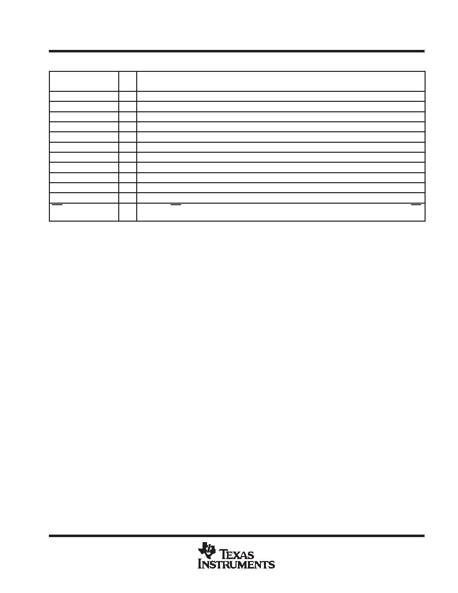
Terminal Functions
TERMINAL
I/O
DESCRIPTION
NAME
NO.
I/O
DESCRIPTION
AGND
5
Analog ground. AGND is the reference and return terminal for the analog signals and supply.
A0, A1
17, 16
I
DAC select inputs. The combination of high or low levels select either DACA, DACB, DACC, or DACD.
DGND
6
Digital ground. DGND is the reference and return terminal for the digital signals and supply.
DB0 DB7
147
I
Digital DAC data inputs. DB0 DB7 are the input digital data used for conversion.
OUTA
2
O
DACA output. OUTA is the analog output of DACA.
OUTB
1
O
DACB output. OUTB is the analog output of DACB.
OUTC
20
O
DACC output. OUTC is the analog output of DACC.
OUTD
19
O
DACD output. OUTD is the analog output of DACD.
REF
4
I
Voltage reference input. The voltage level on REF determines the full scale analog output.
VDD
18
Positive supply voltage input terminal
VSS
3
Negative supply voltage input terminal
WR
15
I
Write input. WR selects DAC transparency or latch mode. The selected input latch is transparent when WR
is low.
Terminal numbers shown are for the DW, N, and FK packages.
absolute maximum ratings over operating free-air temperature range (unless otherwise noted)
Supply voltage range, VDD: AGND or DGND
0.3 V to 17 V
. . . . . . . . . . . . . . . . . . . . . . . . . . . . . . . . . . . . . . . . .
VSS
0.3 V to 24 V
. . . . . . . . . . . . . . . . . . . . . . . . . . . . . . . . . . . . . . . . . . . . . . . . . . .
Supply voltage range, VSS: AGND or DGND
7 V to 0.3 V
. . . . . . . . . . . . . . . . . . . . . . . . . . . . . . . . . . . . . . . . . .
Voltage range between AGND and DGND
17 V to 17 V
. . . . . . . . . . . . . . . . . . . . . . . . . . . . . . . . . . . . . . . . . . . .
Input voltage range, VI (to DGND)
0.3 V to VDD + 0.3 V
. . . . . . . . . . . . . . . . . . . . . . . . . . . . . . . . . . . . . . . . . . . .
Reference voltage range: Vref (to AGND)
0.3 V to VDD
. . . . . . . . . . . . . . . . . . . . . . . . . . . . . . . . . . . . . . . . . . .
Vref (to VSS)
0.3 V to 20 V
. . . . . . . . . . . . . . . . . . . . . . . . . . . . . . . . . . . . . . . . . . . . .
Output voltage range, VO (to AGND) (see Note 1)
VSS to VDD
. . . . . . . . . . . . . . . . . . . . . . . . . . . . . . . . . . . . . . . .
Continuous total power dissipation at (or below) TA = 25°C (see Note 2)
500 mW
. . . . . . . . . . . . . . . . . . . . . . .
Operating free-air temperature range, TA: C suffix
0
°C to 70°C
. . . . . . . . . . . . . . . . . . . . . . . . . . . . . . . . . . . . . . .
E suffix
30
°C to 85°C
. . . . . . . . . . . . . . . . . . . . . . . . . . . . . . . . . . . . .
M suffix
55
°C to 125°C
. . . . . . . . . . . . . . . . . . . . . . . . . . . . . . . . . . . .
Storage temperature range, Tstg
65
°C to 150°C
. . . . . . . . . . . . . . . . . . . . . . . . . . . . . . . . . . . . . . . . . . . . . . . . . . .
Case temperature for 10 seconds: FK package
260
°C
. . . . . . . . . . . . . . . . . . . . . . . . . . . . . . . . . . . . . . . . . . . . . .
Stresses beyond those listed under “absolute maximum ratings” may cause permanent damage to the device. These are stress ratings only, and
functional operation of the device at these or any other conditions beyond those indicated under “recommended operating conditions” is not
implied. Exposure to absolute-maximum-rated conditions for extended periods may affect device reliability.
The VSS terminal is connected to the substrate and must be tied to the most negative supply voltage applied to the device.
NOTES:
1. Output voltages may be shorted to AGND provided that the power dissipation of the package is not exceeded. Typically short circuit
current to AGND is 60 mA.
2. For operation above TA = 75°C, derate linearly at the rate of 2 mW/°C.
相关PDF资料 |
PDF描述 |
|---|---|
| TLC7226IDWG4 | PARALLEL, 8 BITS INPUT LOADING, 7 us SETTLING TIME, 8-BIT DAC, PDSO20 |
| TLC7226CN | PARALLEL, 8 BITS INPUT LOADING, 7 us SETTLING TIME, 8-BIT DAC, PDIP20 |
| TLC7226IDWRG4 | PARALLEL, 8 BITS INPUT LOADING, 7 us SETTLING TIME, 8-BIT DAC, PDSO20 |
| TLC7226INE4 | PARALLEL, 8 BITS INPUT LOADING, 7 us SETTLING TIME, 8-BIT DAC, PDIP20 |
| TLC7226IN | PARALLEL, 8 BITS INPUT LOADING, 7 us SETTLING TIME, 8-BIT DAC, PDIP20 |
相关代理商/技术参数 |
参数描述 |
|---|---|
| TLC7226I | 制造商:TI 制造商全称:Texas Instruments 功能描述:QUADRUPLE 8-BIT DIGITAL-TO-ANALOG CONVERTERS |
| TLC7226IDW | 功能描述:数模转换器- DAC Quad DAC 8bit RoHS:否 制造商:Texas Instruments 转换器数量:1 DAC 输出端数量:1 转换速率:2 MSPs 分辨率:16 bit 接口类型:QSPI, SPI, Serial (3-Wire, Microwire) 稳定时间:1 us 最大工作温度:+ 85 C 安装风格:SMD/SMT 封装 / 箱体:SOIC-14 封装:Tube |
| TLC7226IDWG4 | 功能描述:数模转换器- DAC Quad Parallel-In Sngl/Dual Sply RoHS:否 制造商:Texas Instruments 转换器数量:1 DAC 输出端数量:1 转换速率:2 MSPs 分辨率:16 bit 接口类型:QSPI, SPI, Serial (3-Wire, Microwire) 稳定时间:1 us 最大工作温度:+ 85 C 安装风格:SMD/SMT 封装 / 箱体:SOIC-14 封装:Tube |
| TLC7226IDWR | 功能描述:数模转换器- DAC Quad Parallel-In Sngl/Dual Sply RoHS:否 制造商:Texas Instruments 转换器数量:1 DAC 输出端数量:1 转换速率:2 MSPs 分辨率:16 bit 接口类型:QSPI, SPI, Serial (3-Wire, Microwire) 稳定时间:1 us 最大工作温度:+ 85 C 安装风格:SMD/SMT 封装 / 箱体:SOIC-14 封装:Tube |
| TLC7226IDWRG4 | 功能描述:数模转换器- DAC Quad Parallel-In Sngl/Dual Sply RoHS:否 制造商:Texas Instruments 转换器数量:1 DAC 输出端数量:1 转换速率:2 MSPs 分辨率:16 bit 接口类型:QSPI, SPI, Serial (3-Wire, Microwire) 稳定时间:1 us 最大工作温度:+ 85 C 安装风格:SMD/SMT 封装 / 箱体:SOIC-14 封装:Tube |
发布紧急采购,3分钟左右您将得到回复。