- 您现在的位置:买卖IC网 > PDF目录382606 > TLC8188 (Texas Instruments, Inc.) 10-Bit, 4 MSPS, CIS/Linear CCD Sensor Processor(10位,4MSPS,CIS/线性CCD传感处理器) PDF资料下载
参数资料
| 型号: | TLC8188 |
| 厂商: | Texas Instruments, Inc. |
| 英文描述: | 10-Bit, 4 MSPS, CIS/Linear CCD Sensor Processor(10位,4MSPS,CIS/线性CCD传感处理器) |
| 中文描述: | 10位,4 MSPS的,独联体/线性CCD传感器处理器(10位,4MSPS,独联体/线性防治荒漠化公约传感处理器) |
| 文件页数: | 10/12页 |
| 文件大小: | 153K |
| 代理商: | TLC8188 |
TLC8188
10-BIT, 4 MSPS, CIS/LINEAR CCD SENSOR PROCESSOR
SLAS177A – DECEMBER 1997 – REVISED SEPTEMBER 1998
10
POST OFFICE BOX 655303
DALLAS, TEXAS 75265
PRINCIPLES OF OPERATION
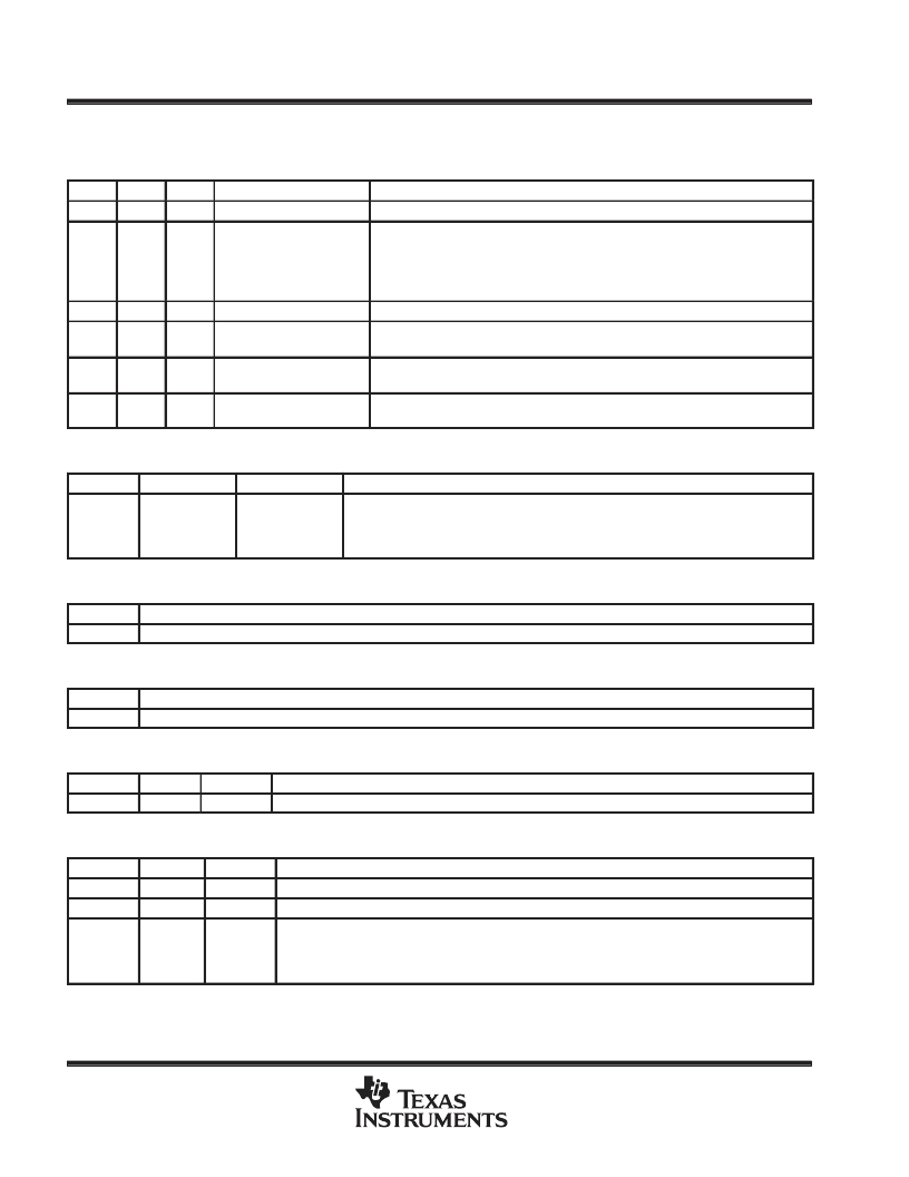
color selection mode description
FME
MM1
MM0
NAME
DESCRIPTION
0
0
0
Internal, no force mux
Input mux, offset and gain register selected from internal register bits INTM1, INTM0
0
0
1
External, no force mux
Input mux, offset and gain register selected from external pins MA1, MA0
MA1
MA0
0
0
Red
0
1
Green
1
0
Blue
0
1
0
Auto-cycling, no force mux
Input mux, offset and gain register auto-cycled, R
→
G
→
B
→
R on ACYC pulse.
Input mux selected from internal register bits FM1, FM0; offset and gain register
selected from internal register bits INTM1, INTM0
1
0
0
Internal, force mux
1
0
1
External, force mux
Input mux selected from internal register bits FM1, FM0; offset and gain register
selected from external pins MA1, MA0
1
1
0
Auto-cycling, force mux
Input mux selected from internal register bits FM1, FM0; offset and gain register
auto-cycled, R
→
G
→
B
→
R on ACYC pulse
setup register 3 description
BIT
NAME
DEFAULT
DESCRIPTION
B1, B0
RCL1, RCL0
No default setting
These two bits control the input clamp voltage levels.
RCL1
RCL0
0
0
0
1
Clamp low, 1.5 V
Clamp high, 2.5 V
software reset description
BIT
DESCRIPTION
B7–B0
Software reset, reset system to the default settings.
auto-cycle reset description
BIT
DESCRIPTION
B7–B0
In auto-cycling mode this will reset auto-cycling to RED channel, RED gain register, and RED offset register.
read-only I.D. description
BIT
NAME
DEFAULT
DESCRIPTION
B7–B0
ID
Hard-coded device revision identification. This can be read in one of the test modes.
test register description
BIT
NAME
DEFAULT
DESCRIPTION
B5–B0
RA5–RA0
00
These six bits select the internal register to be read out at the output data bus.
B7
ST
0
Self test. 1 – self-test enable, the DAC output is connected to the PGA input. 0 – self-test disable (default)
B6
RR
0
Read internal register value from the output data bus. 1 – read enable, 0 – read disable (default). When
the RR bit is set to 1, the content of a register specified by RA5–RA0 can be read from the parallel data
bus upper 8 bits, OP(9–2). Both the parallel and serial ports can be used to write any internal registers,
but only the parallel port is used to read the registers.
相关PDF资料 |
PDF描述 |
|---|---|
| TLE2021AMD | EXCALIBUR HIGH-SPEED LOW-POWER PRECISION OPERATIONAL AMPLIFIERS |
| TLE2021MFKB | EXCALIBUR HIGH-SPEED LOW-POWER PRECISION OPERATIONAL AMPLIFIERS |
| TLE202X | Precision Low-Power Single Supply Operational Amplifier Family |
| TLE202XA | Excalibur High-Speed Low-Power Precision Operational Amplifier Family |
| TLE202XB | Excalibur High-Speed Low-Power Precision Operational Amplifier Family |
相关代理商/技术参数 |
参数描述 |
|---|---|
| TLC8188DA | 制造商:TI 制造商全称:Texas Instruments 功能描述:10-BIT, 4 MSPS, CIS/LINEAR CCD SENSOR PROCESSOR |
| TLC8216FIPW-P | 制造商:Texas Instruments 功能描述: |
| TLC833 | 制造商:ITI 功能描述:833 |
| TLC876 | 制造商:TI 制造商全称:Texas Instruments 功能描述:10-BIT 20 MSPS PARALLEL OUTPUT CMOS ANALOG-TO-DIGITAL CONVERTERS |
| TLC876C | 制造商:TI 制造商全称:Texas Instruments 功能描述:10-BIT 20 MSPS PARALLEL OUTPUT CMOS ANALOG-TO-DIGITAL CONVERTERS |
发布紧急采购,3分钟左右您将得到回复。