- 您现在的位置:买卖IC网 > PDF目录98248 > TLV1508IPWG4 (TEXAS INSTRUMENTS INC) 8-CH 10-BIT SUCCESSIVE APPROXIMATION ADC, SERIAL ACCESS, PDSO20 PDF资料下载
参数资料
| 型号: | TLV1508IPWG4 |
| 厂商: | TEXAS INSTRUMENTS INC |
| 元件分类: | ADC |
| 英文描述: | 8-CH 10-BIT SUCCESSIVE APPROXIMATION ADC, SERIAL ACCESS, PDSO20 |
| 封装: | GREEN, PLASTIC, TSSOP-20 |
| 文件页数: | 23/46页 |
| 文件大小: | 1065K |
| 代理商: | TLV1508IPWG4 |
第1页第2页第3页第4页第5页第6页第7页第8页第9页第10页第11页第12页第13页第14页第15页第16页第17页第18页第19页第20页第21页第22页当前第23页第24页第25页第26页第27页第28页第29页第30页第31页第32页第33页第34页第35页第36页第37页第38页第39页第40页第41页第42页第43页第44页第45页第46页
TLV1504, TLV1508
2.7V TO 5.5V, 10BIT, 200KSPS, 4/8CHANNEL, LOW POWER
SERIAL ANALOGTODIGITAL CONVERTERS WITH AUTOPOWERDOWN
SLAS251A DECEMBER 1999 REVISED JANUARY 2003
3
POST OFFICE BOX 655303
DALLAS, TEXAS 75265
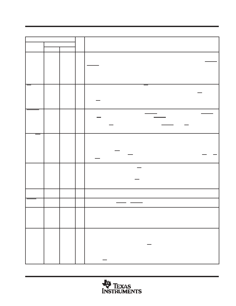
Terminal Functions
TERMINAL
NAME
NO.
I/O
DESCRIPTION
NAME
TLV1504
TLV1508
I/O
DESCRIPTION
A0
A1
A2
A3
A4
A5
A6
A7
6
7
8
9
6
7
8
9
10
11
12
13
I
Analog signal inputs. The analog inputs are applied to these terminals and are internally
multiplexed. The driving source impedance should be less than or equal to 1 k
.
For a source impedance greater than 1 k
, use the asynchronous conversion start signal CSTART
(CSTART low time controls the sampling period) or program long sampling period to increase the
sampling time.
CS
16
20
I
Chip select. A high-to-low transition on the CS input resets the internal 4-bit counter, enables SDI,
and removes SDO from 3-state within a maximum setup time. SDI is disabled within a setup time
after the 4-bit counter counts to 16 (clock edges) or a low-to-high transition of CS whichever
happens first.
NOTE: CS falling and rising edges need to happen when SCLK is low for a microprocessor interface
such as SPI.
CSTART
10
14
I
This terminal controls the start of sampling of the analog input from a selected multiplex channel.
Sampling time starts with the falling edge of CSTART and ends with the rising edge of CSTART as
long as CS is held high. In mode 01, select cycle, CSTART can be issued as soon as CHANNEL
is selected which means the fifth SCLK during the select cycle, but the effective sampling time is
not started until CS goes to high. The rising edge of CSTART (when CS = 1) also starts the
conversion. Tie this terminal to VCC if not used.
EOC/(INT)
4
O
End of conversion or interrupt to host processor.
[PROGRAMMED AS EOC]: This output goes from a high-to-low logic level at the end of the
sampling period and remains low until the conversion is complete and data are ready for transfer.
EOC is used in conversion mode 00 only.
[PROGRAMMED AS INT]: This pin can also be programmed as an interrupt output signal to the host
processor. The falling edge of INT indicates data are ready for output. The following CS
↓ or FS
clears INT.
FS
13
17
I
DSP frame sync input. Indication of the start of a serial data frame in or out of the device. If FS
remains low after the falling edge of CS, SDI is not enabled until an active FS is presented. A
high-to-low transition on the FS input resets the internal 4-bit counter and enables SDI within a
maximum setup time. SDI is disabled within a setup time after the 4-bit counter counts to 16 (clock
edges) or a low-to-high transition of CS whichever happens first.
Tie this terminal to VCC if not used. See the date code information section, item (1).
GND
11
15
I
Ground return for the internal circuitry. Unless otherwise noted, all voltage measurements are with
respect to GND.
PWDN
12
16
I
Both analog and reference circuits are powered down when this pin is at logic zero. The device can
be restarted by active CS, FS or CSTART after this pin is pulled back to logic one.
SCLK
3
I
Input serial clock. This terminal receives the serial SCLK from the host processor. SCLK is used to
clock the input SDI to the input register. When programmed, it may also be used as the source of
the conversion clock.
NOTE: This device supports CPOL (clock polarity) = 0, which is SCLK returns to zero when idling
for SPI compatible interface.
SDI
2
I
Serial data input. The input data is presented with the MSB (D15) first. The first 4-bit MSBs,
D(1512) are decoded as one of the 16 commands (12 only for the TLV1504). The configure write
commands require an additional 12 bits of data.
When FS is not used (FS =1), the first MSB (D15) is expected after the falling edge of CS and is
latched in on the rising edges of SCLK (after CS
↓).
When FS is used (typical with an active FS from a DSP) the first MSB (D15) is expected after the
falling edge of FS and is latched in on the falling edges of SCLK.
SDI is disabled within a setup time after the 4-bit counter counts to 16 (clock edges) or a low-to-high
transition of CS whichever happens first.
相关PDF资料 |
PDF描述 |
|---|---|
| TLV1508IPWRG4 | 8-CH 10-BIT SUCCESSIVE APPROXIMATION ADC, SERIAL ACCESS, PDSO20 |
| TLV1544CPWLE | 4-CH 10-BIT SUCCESSIVE APPROXIMATION ADC, SERIAL ACCESS, PDSO16 |
| TLV1548IDBLE | 8-CH 10-BIT SUCCESSIVE APPROXIMATION ADC, SERIAL ACCESS, PDSO20 |
| TLV1544IPWLE | 4-CH 10-BIT SUCCESSIVE APPROXIMATION ADC, SERIAL ACCESS, PDSO16 |
| TLV1548MFK | 8-CH 10-BIT SUCCESSIVE APPROXIMATION ADC, SERIAL ACCESS, CQCC20 |
相关代理商/技术参数 |
参数描述 |
|---|---|
| TLV1508IPWR | 功能描述:模数转换器 - ADC 10-Bit 200 kSPS Serial Out RoHS:否 制造商:Texas Instruments 通道数量:2 结构:Sigma-Delta 转换速率:125 SPs to 8 KSPs 分辨率:24 bit 输入类型:Differential 信噪比:107 dB 接口类型:SPI 工作电源电压:1.7 V to 3.6 V, 2.7 V to 5.25 V 最大工作温度:+ 85 C 安装风格:SMD/SMT 封装 / 箱体:VQFN-32 |
| TLV1508IPWRG4 | 功能描述:模数转换器 - ADC 10-Bit 200 kSPS Serial Out RoHS:否 制造商:Texas Instruments 通道数量:2 结构:Sigma-Delta 转换速率:125 SPs to 8 KSPs 分辨率:24 bit 输入类型:Differential 信噪比:107 dB 接口类型:SPI 工作电源电压:1.7 V to 3.6 V, 2.7 V to 5.25 V 最大工作温度:+ 85 C 安装风格:SMD/SMT 封装 / 箱体:VQFN-32 |
| TLV1543 | 制造商:TI 制造商全称:Texas Instruments 功能描述:3.3V 10 BIT ANALOG TO DIGITAL CONVERTERS WITH SERIAL CONTROL AND 11 ANALOG INPUTS |
| TLV1543C | 制造商:TI 制造商全称:Texas Instruments 功能描述:3.3-V 10-BIT ANALOG-TO-DIGITAL CONVERTERS WITH SERIAL CONTROL AND 11 ANALOG INPUTS |
| TLV1543CDB | 功能描述:模数转换器 - ADC High Speed A/D RoHS:否 制造商:Texas Instruments 通道数量:2 结构:Sigma-Delta 转换速率:125 SPs to 8 KSPs 分辨率:24 bit 输入类型:Differential 信噪比:107 dB 接口类型:SPI 工作电源电压:1.7 V to 3.6 V, 2.7 V to 5.25 V 最大工作温度:+ 85 C 安装风格:SMD/SMT 封装 / 箱体:VQFN-32 |
发布紧急采购,3分钟左右您将得到回复。