- 您现在的位置:买卖IC网 > PDF目录10462 > TLV1549IPE4 (Texas Instruments)IC 10 BIT 38 KSPS ADC S/O 8-DIP PDF资料下载
参数资料
| 型号: | TLV1549IPE4 |
| 厂商: | Texas Instruments |
| 文件页数: | 16/19页 |
| 文件大小: | 0K |
| 描述: | IC 10 BIT 38 KSPS ADC S/O 8-DIP |
| 产品培训模块: | Data Converter Basics |
| 标准包装: | 50 |
| 位数: | 10 |
| 采样率(每秒): | 38k |
| 数据接口: | 串行 |
| 转换器数目: | 1 |
| 功率耗散(最大): | 1.32mW |
| 电压电源: | 单电源 |
| 工作温度: | -40°C ~ 85°C |
| 安装类型: | 通孔 |
| 封装/外壳: | 8-DIP(0.300",7.62mm) |
| 供应商设备封装: | 8-PDIP |
| 包装: | 管件 |
| 输入数目和类型: | 1 个单端,单极 |
TLV1549C, TLV1549I, TLV1549M
10-BIT ANALOG-TO-DIGITAL CONVERTERS
WITH SERIAL CONTROL
SLAS071C – JANUARY 1993 – REVISED MARCH 1995
6
POST OFFICE BOX 655303
DALLAS, TEXAS 75265
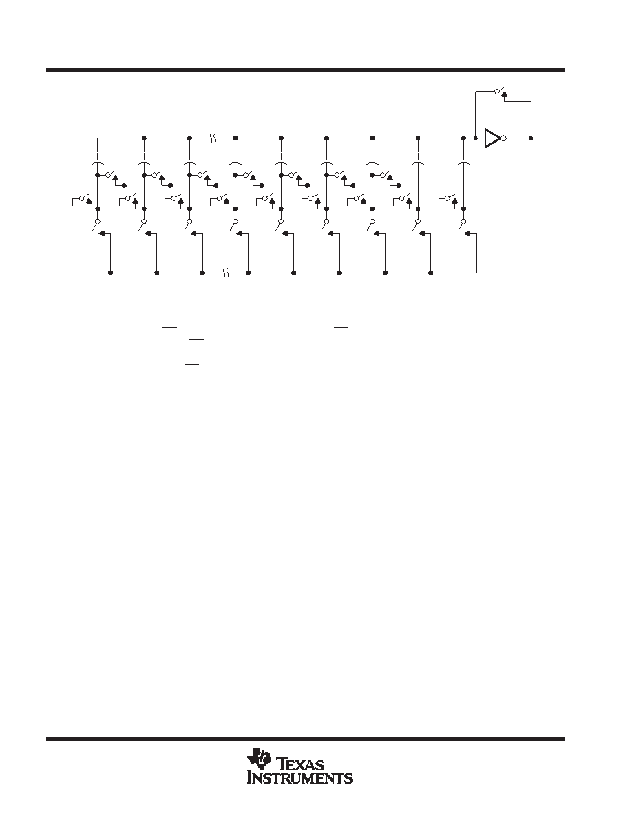
SC
Threshold
Detector
NODE 512
REF –
REF+
ST
512
VI
To Output
Latches
1
2
4
8
16
128
256
REF+
REF –
ST
Figure 1. Simplified Model of the Successive-Approximation System
chip-select operation
The trailing edge of CS starts all modes of operation, and CS can abort a conversion sequence in any mode.
A high-to-low transition on CS within the specified time during an ongoing cycle aborts the cycle, and the device
returns to the initial state (the contents of the output data register remain at the previous conversion result).
Exercise care to prevent CS from being taken low close to completion of conversion because the output data
may be corrupted.
reference voltage inputs
There are two reference inputs used with the TLV1549: REF+ and REF–. These voltage values establish the
upper and lower limits of the analog input to produce a full-scale and zero reading, respectively. The values of
REF+, REF–, and the analog input should not exceed the positive supply or be lower than GND consistent with
the specified absolute maximum ratings. The digital output is at full scale when the input signal is equal to or
higher than REF+ and at zero when the input signal is equal to or lower than REF–.
absolute maximum ratings over operating free-air temperature range (unless otherwise noted)
Supply voltage range, VCC (see Note 1): TLV1549C
–0.5 V to 6.5 V
. . . . . . . . . . . . . . . . . . . . . . . . . . . . . . . . . .
TLV1549I
–0.5 V to 6.5 V
. . . . . . . . . . . . . . . . . . . . . . . . . . . . . . . . . . .
TLV1549M
–0.5 V to 6 V
. . . . . . . . . . . . . . . . . . . . . . . . . . . . . . . . . . .
Input voltage range, VI (any input)
–0.3 V to VCC + 0.3 V
. . . . . . . . . . . . . . . . . . . . . . . . . . . . . . . . . . . . . . . . . . . .
Output voltage range, VO
–0.3 V to VCC + 0.3 V
. . . . . . . . . . . . . . . . . . . . . . . . . . . . . . . . . . . . . . . . . . . . . . . . . . .
Positive reference voltage, Vref+
VCC + 0.1 V
. . . . . . . . . . . . . . . . . . . . . . . . . . . . . . . . . . . . . . . . . . . . . . . . . . . . . .
Negative reference voltage, Vref–
–0.1 V
. . . . . . . . . . . . . . . . . . . . . . . . . . . . . . . . . . . . . . . . . . . . . . . . . . . . . . . . . .
Peak input current (any input)
±20 mA
. . . . . . . . . . . . . . . . . . . . . . . . . . . . . . . . . . . . . . . . . . . . . . . . . . . . . . . . . . . .
Peak total input current (all inputs)
±30 mA
. . . . . . . . . . . . . . . . . . . . . . . . . . . . . . . . . . . . . . . . . . . . . . . . . . . . . . . .
Operating free-air temperature range, TA: TLV1549C
0
°C to 70°C
. . . . . . . . . . . . . . . . . . . . . . . . . . . . . . . . . . .
TLV1549I
–40
°C to 85°C
. . . . . . . . . . . . . . . . . . . . . . . . . . . . . . . . . .
TLV1549M
–55
°C to 125°C
. . . . . . . . . . . . . . . . . . . . . . . . . . . . . . . .
Storage temperature range, Tstg
–65
°C to 150°C
. . . . . . . . . . . . . . . . . . . . . . . . . . . . . . . . . . . . . . . . . . . . . . . . . . .
Lead temperature 1,6 mm (1/16 inch) from the case for 10 seconds
260
°C
. . . . . . . . . . . . . . . . . . . . . . . . . . . .
Stresses beyond those listed under “absolute maximum ratings” may cause permanent damage to the device. These are stress ratings only, and
functional operation of the device at these or any other conditions beyond those indicated under “recommended operating conditions” is not
implied. Exposure to absolute-maximum-rated conditions for extended periods may affect device reliability.
NOTE 1: All voltage values are with respect to ground with REF – and GND wired together (unless otherwise noted).
相关PDF资料 |
PDF描述 |
|---|---|
| VI-210-IU | CONVERTER MOD DC/DC 5V 200W |
| VJ1812Y101KXEAT5Z | CAP CER 100PF 500V 10% X7R 1812 |
| VI-26W-IV-B1 | CONVERTER MOD DC/DC 5.5V 150W |
| VE-210-IW-F3 | CONVERTER MOD DC/DC 5V 100W |
| VE-210-IW-F1 | CONVERTER MOD DC/DC 5V 100W |
相关代理商/技术参数 |
参数描述 |
|---|---|
| TLV1549M | 制造商:TI 制造商全称:Texas Instruments 功能描述:10-BIT ANALOG-TO-DIGITAL CONVERTERS WITH SERIAL CONTROL |
| TLV1549MFK | 制造商:TI 制造商全称:Texas Instruments 功能描述:10-BIT ANALOG-TO-DIGITAL CONVERTERS WITH SERIAL CONTROL |
| TLV1549MJG | 制造商:TI 制造商全称:Texas Instruments 功能描述:10-BIT ANALOG-TO-DIGITAL CONVERTERS WITH SERIAL CONTROL |
| TLV1562 | 制造商:TI 制造商全称:Texas Instruments 功能描述:2.7 V TO 5.5 V, HIGH-SPEED LOW-POWER RECONFIGURABLE ANALOG-TO-DIGITAL CONVERTER WITH 4-INPUT, DUAL S/H, PARALLEL INTERFACE, AND POWER DOWN |
| TLV1562CDW | 功能描述:模数转换器 - ADC 10bit Programmable RoHS:否 制造商:Texas Instruments 通道数量:2 结构:Sigma-Delta 转换速率:125 SPs to 8 KSPs 分辨率:24 bit 输入类型:Differential 信噪比:107 dB 接口类型:SPI 工作电源电压:1.7 V to 3.6 V, 2.7 V to 5.25 V 最大工作温度:+ 85 C 安装风格:SMD/SMT 封装 / 箱体:VQFN-32 |
发布紧急采购,3分钟左右您将得到回复。