- 您现在的位置:买卖IC网 > PDF目录98249 > TLV1562IDWR (TEXAS INSTRUMENTS INC) 4-CH 10-BIT PROPRIETARY METHOD ADC, PARALLEL ACCESS, PDSO28 PDF资料下载
参数资料
| 型号: | TLV1562IDWR |
| 厂商: | TEXAS INSTRUMENTS INC |
| 元件分类: | ADC |
| 英文描述: | 4-CH 10-BIT PROPRIETARY METHOD ADC, PARALLEL ACCESS, PDSO28 |
| 封装: | 1.27 MM PITCH, GREEN, SOIC-28 |
| 文件页数: | 10/41页 |
| 文件大小: | 600K |
| 代理商: | TLV1562IDWR |
第1页第2页第3页第4页第5页第6页第7页第8页第9页当前第10页第11页第12页第13页第14页第15页第16页第17页第18页第19页第20页第21页第22页第23页第24页第25页第26页第27页第28页第29页第30页第31页第32页第33页第34页第35页第36页第37页第38页第39页第40页第41页
TLV1562
2.7 V TO 5.5 V, HIGH-SPEED LOW-POWER RECONFIGURABLE ANALOG-TO-DIGITAL
CONVERTER WITH 4-INPUT, DUAL S/H, PARALLEL INTERFACE, AND POWER DOWN
SLAS162 – SEPTEMBER 1998
18
POST OFFICE BOX 655303
DALLAS, TEXAS 75265
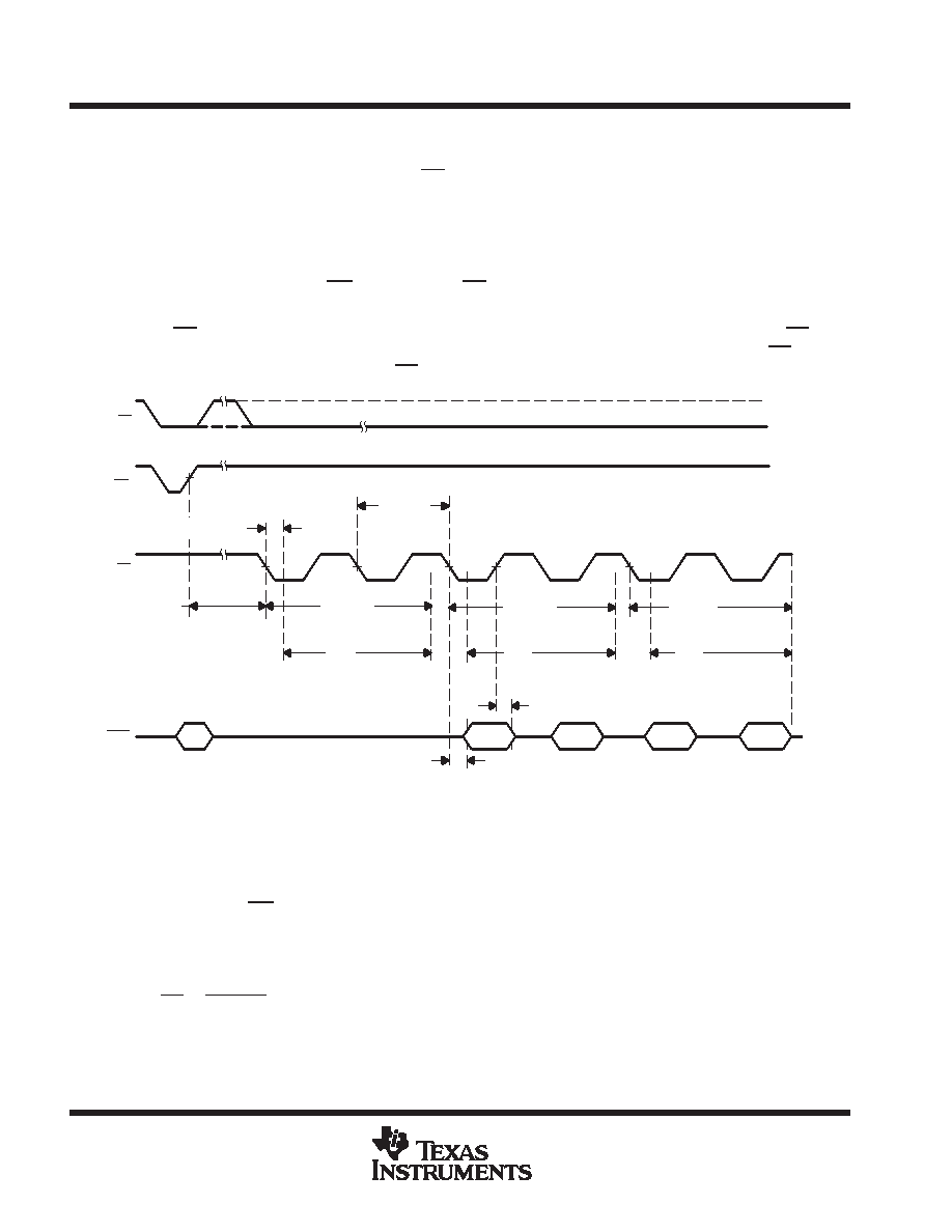
dual continuous mode (CR0.(3,2) = 1,1)
When the TLV1562 operates in the dual continuous mode, it samples and then holds two preselected channels
(differential or single ended) simultaneously as RD clocks. These samples are then converted in sequence. This
is designed to optimize the DSP MIPS for communication applications. Its cycle time is approximately 10
SYSCLK cycles when an external SYSCLK is used (12 SYSCLK cycles when an internal SYSCLK is used).
When operating in the dual continuous mode, the TLV1562 is always sampling the input regardless of the state
of the other control signals when it is not in the hold state. This simplifies control of the ADC. There is no need
to generate any special signal to start the sampling. The TLV1562 goes into hold mode on the odd number
(starting from the rising edge of WR) falling edge of RD for one SYSCLK clock cycle.
A two-depth FIFO is used (only in the dual continuous mode) to ensure the output correlation. Thus on every
alternate RD edge, the result of the previous two conversions is read out. This allows a slower RD clock
frequency (slower than 1/5 of the SYSCLK frequency). Each dual continuous mode cycle (while CS remains
active low) must have an even number of RD cycles to ensure the FIFO operates properly.
CS
WR
RD
DATA
t dis(DATAOUT)
t en(DATAOUT)
t d(RDL-SAMPLE)
t c(RD)
t s5
tconv2
t conv2
CONV 1
CONV 2
CONV 3
t s3
Sample 2
t s3
Sample 3
t s3
Sample 4
D 1A
D 1B
D 2A
GFG
Sample 1
D 2B
VIH
VIL
Figure 15. Dual Continuous Mode
system clock source
The TLV1562 uses multiple clocks for different internal tasks. SYSCLK is used for most conversion subtasks.
The source of SYSCLK is programmable via control register 0, bit 5 (CR0.5). The source of SYSCLK is changed
at the rising edge of WR of the cycle when CR0.5 is programmed.
internal oscillator (CR0.5 = 0, SYSCLK = internal OSC)
The TLV1562 has a built-in 8-MHz oscillator. When the internal OSC is selected as the source of SYSCLK, the
internal clock starts with a delay (one half of the OSC clock period max) after the falling edge of the conversion
trigger (RD or CSTART).
相关PDF资料 |
PDF描述 |
|---|---|
| TLV1562CPWR | 4-CH 10-BIT PROPRIETARY METHOD ADC, PARALLEL ACCESS, PDSO28 |
| TLV1562CPW | 4-CH 10-BIT PROPRIETARY METHOD ADC, PARALLEL ACCESS, PDSO28 |
| TLV1562IPWR | 4-CH 10-BIT PROPRIETARY METHOD ADC, PARALLEL ACCESS, PDSO28 |
| TLV1562IPW | 4-CH 10-BIT PROPRIETARY METHOD ADC, PARALLEL ACCESS, PDSO28 |
| TLV1562CPWG4 | 4-CH 10-BIT PROPRIETARY METHOD ADC, PARALLEL ACCESS, PDSO28 |
相关代理商/技术参数 |
参数描述 |
|---|---|
| TLV1562IDWRG4 | 功能描述:模数转换器 - ADC 10-Bit 2 MSPS Quad Channel RoHS:否 制造商:Texas Instruments 通道数量:2 结构:Sigma-Delta 转换速率:125 SPs to 8 KSPs 分辨率:24 bit 输入类型:Differential 信噪比:107 dB 接口类型:SPI 工作电源电压:1.7 V to 3.6 V, 2.7 V to 5.25 V 最大工作温度:+ 85 C 安装风格:SMD/SMT 封装 / 箱体:VQFN-32 |
| TLV1562IPW | 功能描述:模数转换器 - ADC 10bit Programmable RoHS:否 制造商:Texas Instruments 通道数量:2 结构:Sigma-Delta 转换速率:125 SPs to 8 KSPs 分辨率:24 bit 输入类型:Differential 信噪比:107 dB 接口类型:SPI 工作电源电压:1.7 V to 3.6 V, 2.7 V to 5.25 V 最大工作温度:+ 85 C 安装风格:SMD/SMT 封装 / 箱体:VQFN-32 |
| TLV1562IPWG4 | 功能描述:模数转换器 - ADC 10-Bit 2 MSPS Quad Channel RoHS:否 制造商:Texas Instruments 通道数量:2 结构:Sigma-Delta 转换速率:125 SPs to 8 KSPs 分辨率:24 bit 输入类型:Differential 信噪比:107 dB 接口类型:SPI 工作电源电压:1.7 V to 3.6 V, 2.7 V to 5.25 V 最大工作温度:+ 85 C 安装风格:SMD/SMT 封装 / 箱体:VQFN-32 |
| TLV1570 | 制造商:TI 制造商全称:Texas Instruments 功能描述:2.7 V TO 5.5 V 8-CHANNEL 10-BIT 1.25-MSPS SERIAL ANALOG-TO-DIGITAL CONVERTER |
| TLV1570CDW | 功能描述:模数转换器 - ADC 10bit 1.25MSPS Ser RoHS:否 制造商:Texas Instruments 通道数量:2 结构:Sigma-Delta 转换速率:125 SPs to 8 KSPs 分辨率:24 bit 输入类型:Differential 信噪比:107 dB 接口类型:SPI 工作电源电压:1.7 V to 3.6 V, 2.7 V to 5.25 V 最大工作温度:+ 85 C 安装风格:SMD/SMT 封装 / 箱体:VQFN-32 |
发布紧急采购,3分钟左右您将得到回复。