- 您现在的位置:买卖IC网 > PDF目录98250 > TLV2541CDGKG4 (TEXAS INSTRUMENTS INC) 1-CH 12-BIT SUCCESSIVE APPROXIMATION ADC, SERIAL ACCESS, PDSO8 PDF资料下载
参数资料
| 型号: | TLV2541CDGKG4 |
| 厂商: | TEXAS INSTRUMENTS INC |
| 元件分类: | ADC |
| 英文描述: | 1-CH 12-BIT SUCCESSIVE APPROXIMATION ADC, SERIAL ACCESS, PDSO8 |
| 封装: | GREEN, PLASTIC, MSOP-8 |
| 文件页数: | 26/31页 |
| 文件大小: | 778K |
| 代理商: | TLV2541CDGKG4 |
第1页第2页第3页第4页第5页第6页第7页第8页第9页第10页第11页第12页第13页第14页第15页第16页第17页第18页第19页第20页第21页第22页第23页第24页第25页当前第26页第27页第28页第29页第30页第31页
TLV2541, TLV2542, TLV2545
2.7-V TO 5.5-V, LOW-POWER, 12-BIT, 140/200 KSPS,
SERIAL ANALOG-TO-DIGITAL CONVERTERS WITH AUTOPOWER DOWN
SLAS245E MARCH 2000 REVISED APRIL 2010
4
POST OFFICE BOX 655303
DALLAS, TEXAS 75265
POST OFFICE BOX 1443
HOUSTON, TEXAS 772511443
detailed description (continued)
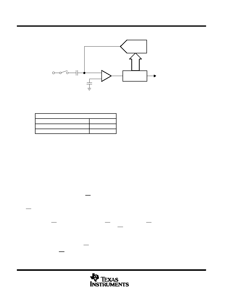
GND/AIN()
ADC Code
AIN
Charge
Redistribution
DAC
Control
Logic
_
+
Figure 1. Simplified SAR Circuit
serial interface
OUTPUT DATA FORMAT
MSB
LSB
D15D4
D3D0
Conversion result (OD11OD0)
Don’t care
The output data format is binary (unipolar straight binary).
binary
Zero-scale code = 000h, Vcode = GND
Full-scale code = FFFh, Vcode = VREF 1 LSB
pseudo-differential inputs
The TLV2545 operates in pseudo-differential mode. The inverted input is available on pin 5. It can have a
maximum input ripple of ±0.2 V. This is normally used for ground noise rejection.
control and timing
start of the cycle
Each cycle may be started by either CS, FS, or a combination of both. The internal state machine requires one
SCLK high-to-low transition to determine the state of these control signals so internal blocks can be powered
up in an active cycle. Special care to SPI mode is necessary. Make sure there is at least one SCLK whenever
CS (pin 1) is high to ensure proper operation.
TLV2541
D Control via CS ( FS = 1 at the falling edge of CS)—The falling edge of CS is the start of the cycle. The MSB
should be read on the first falling SCLK edge after CS is low. Output data changes on the rising edge of
SCLK. This is typically used for a microcontroller with an SPI interface, although it can also be used for a
DSP. The microcontroller SPI interface should be programmed for CPOL = 0 (serial clock referenced to
ground) and CPHA = 1 (data is valid on the falling edge of the serial clock). At least one falling edge transition
on SCLK is needed whenever CS is brought high.
D Control via FS (CS is tied/held low)—The MSB is presented after the rising edge of FS. The falling edge
of FS is the start of the cycle. The MSB should be read on the first falling edge of SCLK after FS is low. This
is the typical configuration when the ADC is the only device on the DSP serial port.
相关PDF资料 |
PDF描述 |
|---|---|
| TLV2541IDGKG4 | 1-CH 12-BIT SUCCESSIVE APPROXIMATION ADC, SERIAL ACCESS, PDSO8 |
| TLV2541IDGK | 1-CH 12-BIT SUCCESSIVE APPROXIMATION ADC, SERIAL ACCESS, PDSO8 |
| TLV2541IDGKR | 1-CH 12-BIT SUCCESSIVE APPROXIMATION ADC, SERIAL ACCESS, PDSO8 |
| TLV2542IDRG4 | 2-CH 12-BIT SUCCESSIVE APPROXIMATION ADC, SERIAL ACCESS, PDSO8 |
| TLV2543CDBLE | 11-CH 12-BIT SUCCESSIVE APPROXIMATION ADC, SERIAL ACCESS, PDSO20 |
相关代理商/技术参数 |
参数描述 |
|---|---|
| TLV2541CDGKR | 功能描述:模数转换器 - ADC 12-Bit 200 kSPS Serial Out RoHS:否 制造商:Texas Instruments 通道数量:2 结构:Sigma-Delta 转换速率:125 SPs to 8 KSPs 分辨率:24 bit 输入类型:Differential 信噪比:107 dB 接口类型:SPI 工作电源电压:1.7 V to 3.6 V, 2.7 V to 5.25 V 最大工作温度:+ 85 C 安装风格:SMD/SMT 封装 / 箱体:VQFN-32 |
| TLV2541CDGKRG4 | 功能描述:模数转换器 - ADC 12-Bit 200 kSPS Serial Out RoHS:否 制造商:Texas Instruments 通道数量:2 结构:Sigma-Delta 转换速率:125 SPs to 8 KSPs 分辨率:24 bit 输入类型:Differential 信噪比:107 dB 接口类型:SPI 工作电源电压:1.7 V to 3.6 V, 2.7 V to 5.25 V 最大工作温度:+ 85 C 安装风格:SMD/SMT 封装 / 箱体:VQFN-32 |
| TLV2541EVM | 功能描述:数据转换 IC 开发工具 TLV2541 Eval Mod RoHS:否 制造商:Texas Instruments 产品:Demonstration Kits 类型:ADC 工具用于评估:ADS130E08 接口类型:SPI 工作电源电压:- 6 V to + 6 V |
| TLV2541ID | 功能描述:模数转换器 - ADC 12bit SAR ADC RoHS:否 制造商:Texas Instruments 通道数量:2 结构:Sigma-Delta 转换速率:125 SPs to 8 KSPs 分辨率:24 bit 输入类型:Differential 信噪比:107 dB 接口类型:SPI 工作电源电压:1.7 V to 3.6 V, 2.7 V to 5.25 V 最大工作温度:+ 85 C 安装风格:SMD/SMT 封装 / 箱体:VQFN-32 |
| TLV2541IDG4 | 功能描述:模数转换器 - ADC 12-Bit 200 kSPS Serial Out RoHS:否 制造商:Texas Instruments 通道数量:2 结构:Sigma-Delta 转换速率:125 SPs to 8 KSPs 分辨率:24 bit 输入类型:Differential 信噪比:107 dB 接口类型:SPI 工作电源电压:1.7 V to 3.6 V, 2.7 V to 5.25 V 最大工作温度:+ 85 C 安装风格:SMD/SMT 封装 / 箱体:VQFN-32 |
发布紧急采购,3分钟左右您将得到回复。