- 您现在的位置:买卖IC网 > PDF目录98251 > TLV2544IPWR (TEXAS INSTRUMENTS INC) 4-CH 12-BIT SUCCESSIVE APPROXIMATION ADC, SERIAL ACCESS, PDSO16 PDF资料下载
参数资料
| 型号: | TLV2544IPWR |
| 厂商: | TEXAS INSTRUMENTS INC |
| 元件分类: | ADC |
| 英文描述: | 4-CH 12-BIT SUCCESSIVE APPROXIMATION ADC, SERIAL ACCESS, PDSO16 |
| 封装: | GREEN, PLASTIC, TSSOP-16 |
| 文件页数: | 45/46页 |
| 文件大小: | 1078K |
| 代理商: | TLV2544IPWR |
第1页第2页第3页第4页第5页第6页第7页第8页第9页第10页第11页第12页第13页第14页第15页第16页第17页第18页第19页第20页第21页第22页第23页第24页第25页第26页第27页第28页第29页第30页第31页第32页第33页第34页第35页第36页第37页第38页第39页第40页第41页第42页第43页第44页当前第45页第46页
TLV2544, TLV2548
2.7V TO 5.5V, 12BIT, 200KSPS, 4/8CHANNEL, LOW POWER
SERIAL ANALOGTODIGITAL CONVERTERS WITH AUTOPOWERDOWN
SLAS198E FEBRUARY 1999 REVISED JUNE 2003
8
POST OFFICE BOX 655303
DALLAS, TEXAS 75265
normal sampling
When the converter is using normal sampling, the sampling period is programmable. It can be 12 SCLKs (short
sampling) or 24 SCLKs (long sampling). Long sampling helps when SCLK is faster than 10 MHz or when input
source resistance is high.
extended sampling
CSTART An asynchronous (to the SCLK) signal, via dedicated hardware pin, CSTART, can be used in order
to have total control of the sampling period and the start of a conversion. This extended sampling is user-defined
and is totally independent of SCLK. While CS is high, the falling edge of CSTART is the start of the sampling
period and is controlled by the low time of CSTART. The minimum low time for CSTART should be at least equal
to the minimum t(SAMPLE). In a select cycle used in mode 01 (REPEAT MODE), CSTART can be started as soon
as the channel is selected (after the fifth SCLK). In this case the sampling period is not started until CS has
become inactive. Therefore the nonoverlapped CSTART low time must meet the minimum sampling time
requirement. The low-to-high transition of CSTART terminates the sampling period and starts the conversion
period. The conversion clock can also be configured to use either internal OSC or external SCLK. This function
is useful for an application that requires:
D The use of an extended sampling period to accommodate different input source impedance
D The use of a faster I/O clock on the serial port but not enough sampling time is available due to the fixed
number of SCLKs. This could be due to a high input source impedance or due to higher MUX ON resistance
at lower supply voltage.
Once the conversion is complete, the processor can initiate a read cycle by using either the read FIFO command
to read the conversion result or by simply selecting the next channel number for conversion. Since the device
has a valid conversion result in the output buffer, the conversion result is simply presented at the serial data
output. To completely get out of the extended sampling mode, CS must be toggled twice from a high-to-low
transition while CSTART is high. The read cycle mentioned above followed by another configuration cycle of
the ADC qualifies this condition and successfully puts the ADC back to its normal sampling mode. This can be
viewed in Figure 9.
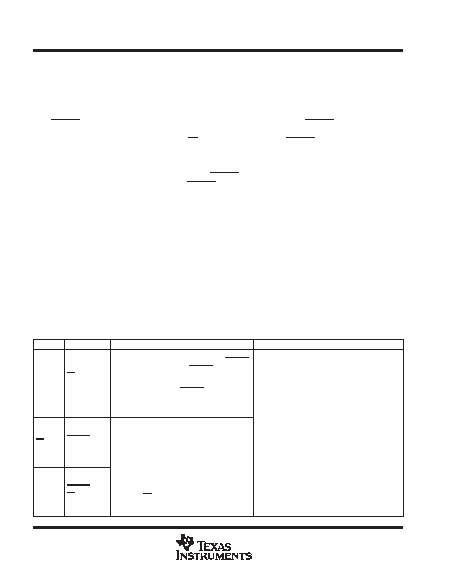
Table 3. Sample and Convert Conditions
CONDITIONS
SAMPLE
CONVERT
CSTART
CS = 1
(see Figures
11 and 18)
No sampling clock (SCLK) required. Sampling
period is totally controlled by the low time of CSTART.
The high-to-low transition of CSTART (when CS=1)
starts the sampling of the analog input signal. The low
time of CSTART dictates the sampling period. The
low-to-high transition of CSTART ends sampling
period and begins the conversion cycle. (Note: this
trigger only works when internal reference is selected
for conversion modes 01, 10, and 11.)
1) If the internal clock OSC is selected a maximum
CS
CSTART = 1
FS = 1
SCLK is required. Sampling period is programmable
under normal sampling. When programmed to sample
under short sampling, 12 SCLKs are generated to
complete sampling period. 24 SCLKs are generated
when programmed for long sampling. A command set
to configure the device requires 4 SCLKs thereby ex-
tending to 16 or 28 SCLKs respectively before conver-
1) If the internal clock OSC is selected a maximum
conversion time of 3.86
s can be achieved.
2) If external SCLK is selected, conversion time is
tconv = 14 × DIV/f(SCLK), where DIV can be 1, 2, or
4.
FS
CSTART = 1
CS = 0
tending to 16 or 28 SCLKs respectively before conver-
sion takes place. (Note: Because the ADC only
bypasses a valid channel select command, the user
can use select channel 0, 0000b, as the SDI input
when either CS or FS is used as trigger for conversion.
The ADC responds to commands such as SW power-
down, 1000b.)
相关PDF资料 |
PDF描述 |
|---|---|
| TLV2548IPWR | 8-CH 12-BIT SUCCESSIVE APPROXIMATION ADC, SERIAL ACCESS, PDSO20 |
| TLV2544ID | 4-CH 12-BIT SUCCESSIVE APPROXIMATION ADC, SERIAL ACCESS, PDSO16 |
| TLV2548IPWLE | 8-CH 12-BIT SUCCESSIVE APPROXIMATION ADC, SERIAL ACCESS, PDSO20 |
| TLV2548CPWLE | 8-CH 12-BIT SUCCESSIVE APPROXIMATION ADC, SERIAL ACCESS, PDSO20 |
| TLV2544IPWLE | 4-CH 12-BIT SUCCESSIVE APPROXIMATION ADC, SERIAL ACCESS, PDSO16 |
相关代理商/技术参数 |
参数描述 |
|---|---|
| TLV2544IPWRG4 | 功能描述:模数转换器 - ADC 12-Bit 200 kSPS Serial Out RoHS:否 制造商:Texas Instruments 通道数量:2 结构:Sigma-Delta 转换速率:125 SPs to 8 KSPs 分辨率:24 bit 输入类型:Differential 信噪比:107 dB 接口类型:SPI 工作电源电压:1.7 V to 3.6 V, 2.7 V to 5.25 V 最大工作温度:+ 85 C 安装风格:SMD/SMT 封装 / 箱体:VQFN-32 |
| TLV2544QD | 功能描述:模数转换器 - ADC 12-Bit 200 kSPS Lo-Pwr RoHS:否 制造商:Texas Instruments 通道数量:2 结构:Sigma-Delta 转换速率:125 SPs to 8 KSPs 分辨率:24 bit 输入类型:Differential 信噪比:107 dB 接口类型:SPI 工作电源电压:1.7 V to 3.6 V, 2.7 V to 5.25 V 最大工作温度:+ 85 C 安装风格:SMD/SMT 封装 / 箱体:VQFN-32 |
| TLV2544QDG4 | 功能描述:模数转换器 - ADC 12B 200 kSPS ADC Ser. Out Lo Pwr RoHS:否 制造商:Texas Instruments 通道数量:2 结构:Sigma-Delta 转换速率:125 SPs to 8 KSPs 分辨率:24 bit 输入类型:Differential 信噪比:107 dB 接口类型:SPI 工作电源电压:1.7 V to 3.6 V, 2.7 V to 5.25 V 最大工作温度:+ 85 C 安装风格:SMD/SMT 封装 / 箱体:VQFN-32 |
| TLV2544QDR | 功能描述:模数转换器 - ADC 12 Bit 200 kSPS Lo Pwr RoHS:否 制造商:Texas Instruments 通道数量:2 结构:Sigma-Delta 转换速率:125 SPs to 8 KSPs 分辨率:24 bit 输入类型:Differential 信噪比:107 dB 接口类型:SPI 工作电源电压:1.7 V to 3.6 V, 2.7 V to 5.25 V 最大工作温度:+ 85 C 安装风格:SMD/SMT 封装 / 箱体:VQFN-32 |
| TLV2544QDRG4 | 功能描述:模数转换器 - ADC 12B 200 kSPS ADC Ser. Out Lo Pwr RoHS:否 制造商:Texas Instruments 通道数量:2 结构:Sigma-Delta 转换速率:125 SPs to 8 KSPs 分辨率:24 bit 输入类型:Differential 信噪比:107 dB 接口类型:SPI 工作电源电压:1.7 V to 3.6 V, 2.7 V to 5.25 V 最大工作温度:+ 85 C 安装风格:SMD/SMT 封装 / 箱体:VQFN-32 |
发布紧急采购,3分钟左右您将得到回复。