- 您现在的位置:买卖IC网 > PDF目录136955 > TLV2772QPWG4 (TEXAS INSTRUMENTS INC) DUAL OP-AMP, 2700 uV OFFSET-MAX, 4.8 MHz BAND WIDTH, PDSO8 PDF资料下载
参数资料
| 型号: | TLV2772QPWG4 |
| 厂商: | TEXAS INSTRUMENTS INC |
| 元件分类: | 运算放大器 |
| 英文描述: | DUAL OP-AMP, 2700 uV OFFSET-MAX, 4.8 MHz BAND WIDTH, PDSO8 |
| 封装: | GREEN, PLASTIC, TSSOP-8 |
| 文件页数: | 30/75页 |
| 文件大小: | 2088K |
| 代理商: | TLV2772QPWG4 |
第1页第2页第3页第4页第5页第6页第7页第8页第9页第10页第11页第12页第13页第14页第15页第16页第17页第18页第19页第20页第21页第22页第23页第24页第25页第26页第27页第28页第29页当前第30页第31页第32页第33页第34页第35页第36页第37页第38页第39页第40页第41页第42页第43页第44页第45页第46页第47页第48页第49页第50页第51页第52页第53页第54页第55页第56页第57页第58页第59页第60页第61页第62页第63页第64页第65页第66页第67页第68页第69页第70页第71页第72页第73页第74页第75页
TLV277x, TLV277xA
FAMILY OF 2.7V HIGHSLEW RATE RAILTORAIL OUTPUT
OPERATIONAL AMPLIFIERS WITH SHUTDOWN
SLOS209G JANUARY 1998 REVISED FEBRUARY 2004
36
WWW.TI.COM
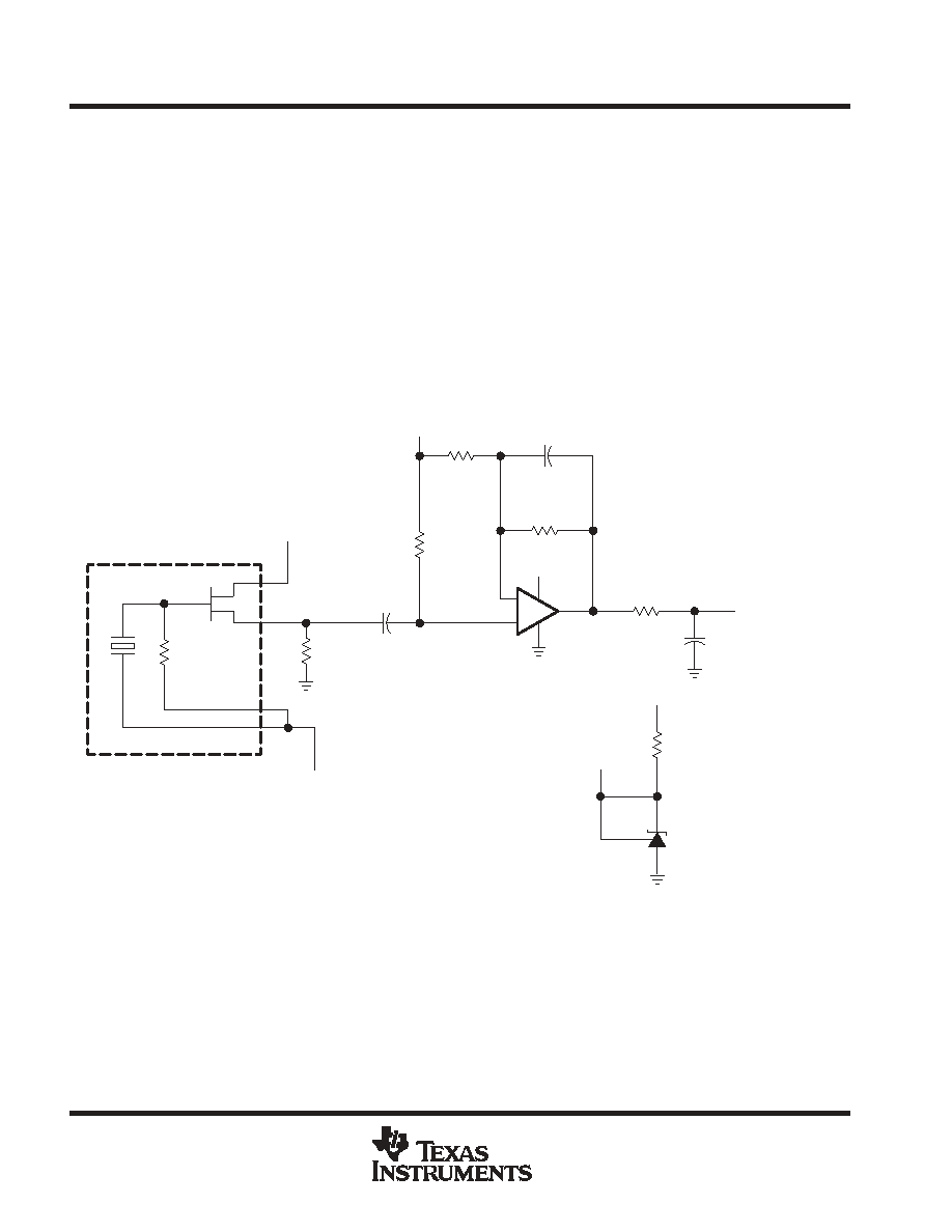
APPLICATION INFORMATION
using the TLV2772 as an accelerometer interface
The schematic, shown in Figure 62, shows the ACH04-08-05 interfaced to the TLV1544 10-bit analog-to-digital
converter (ADC).
The ACH04-08-05 is a shock sensor designed to convert mechanical acceleration into electrical signals. The
sensor contains three piezoelectric sensing elements oriented to simultaneously measure acceleration in three
orthogonal, linear axes (x, y, z). The operating frequency is 0.5 Hz to 5 kHz. The output is buffered with an
internal JFET and has a typical output voltage of 1.80 mV/g for the x and y axis and 1.35 mV/g for the z axis.
Amplification and frequency shaping of the shock sensor output is done by the TLV2772 rail-to-rail operational
amplifier. The TLV2772 is ideal for this application as it offers high input impedance, good slew rate, and
excellent dc precision. The rail-to-rail output swing and high output drive are perfect for driving the analog input
of the TLV1544 ADC.
_
+
1 Axis ACH040805
Shock Sensor
3 V
1.23 V
R1
100 k
C1
0.22
F
R2
1 M
R3
10 k
1.23 V
C2
2.2 nF
R4
100 k
3 V
R5
1 k
C3
0.22
F
1/2
TLV2772
Signal Conditioning
Output to
TLV1544 (ADC)
R6
2.2 k
1.23 V
3 V
TLV431
C
R
A
4
8
1
2
3
Voltage Reference
Figure 62. Accelerometer Interface Schematic
The sensor signal must be amplified and frequency-shaped to provide a signal the ADC can properly convert
into the digital domain. Figure 62 shows the topology used in this application for one axis of the sensor. This
system is powered from a single 3-V supply. Configuring the TLV431 with a 2.2-k
resistor produces a reference
voltage of 1.23 V. This voltage is used to bias the operational amplifier and the internal JFETs in the shock
sensor.
相关PDF资料 |
PDF描述 |
|---|---|
| TLV2772QPWRG4 | DUAL OP-AMP, 2700 uV OFFSET-MAX, 4.8 MHz BAND WIDTH, PDSO8 |
| TL032CPSRG4 | DUAL OP-AMP, 4500 uV OFFSET-MAX, 1 MHz BAND WIDTH, PDSO8 |
| TLV2264AQDG4 | QUAD OP-AMP, 1500 uV OFFSET-MAX, 0.67 MHz BAND WIDTH, PDSO14 |
| TLV2264AQDRG4 | QUAD OP-AMP, 1500 uV OFFSET-MAX, 0.67 MHz BAND WIDTH, PDSO14 |
| TLV2264QDG4 | QUAD OP-AMP, 3000 uV OFFSET-MAX, 0.67 MHz BAND WIDTH, PDSO14 |
相关代理商/技术参数 |
参数描述 |
|---|---|
| TLV2772QPWR | 功能描述:运算放大器 - 运放 Dual 2.7 V High Slew Rate R To R Output RoHS:否 制造商:STMicroelectronics 通道数量:4 共模抑制比(最小值):63 dB 输入补偿电压:1 mV 输入偏流(最大值):10 pA 工作电源电压:2.7 V to 5.5 V 安装风格:SMD/SMT 封装 / 箱体:QFN-16 转换速度:0.89 V/us 关闭:No 输出电流:55 mA 最大工作温度:+ 125 C 封装:Reel |
| TLV2772QPWRG4 | 功能描述:运算放大器 - 运放 Dual 2.7V Hi-Slew Rate Rail to Rail RoHS:否 制造商:STMicroelectronics 通道数量:4 共模抑制比(最小值):63 dB 输入补偿电压:1 mV 输入偏流(最大值):10 pA 工作电源电压:2.7 V to 5.5 V 安装风格:SMD/SMT 封装 / 箱体:QFN-16 转换速度:0.89 V/us 关闭:No 输出电流:55 mA 最大工作温度:+ 125 C 封装:Reel |
| TLV2772QPWRG4Q1 | 功能描述:运算放大器 - 运放 Dual 2.7V Hi-Slew R to R Out Op Amp RoHS:否 制造商:STMicroelectronics 通道数量:4 共模抑制比(最小值):63 dB 输入补偿电压:1 mV 输入偏流(最大值):10 pA 工作电源电压:2.7 V to 5.5 V 安装风格:SMD/SMT 封装 / 箱体:QFN-16 转换速度:0.89 V/us 关闭:No 输出电流:55 mA 最大工作温度:+ 125 C 封装:Reel |
| TLV2772QPWRQ1 | 功能描述:运算放大器 - 运放 Auto Cat 2.7V Hi-Sle Rate Rail to Rail RoHS:否 制造商:STMicroelectronics 通道数量:4 共模抑制比(最小值):63 dB 输入补偿电压:1 mV 输入偏流(最大值):10 pA 工作电源电压:2.7 V to 5.5 V 安装风格:SMD/SMT 封装 / 箱体:QFN-16 转换速度:0.89 V/us 关闭:No 输出电流:55 mA 最大工作温度:+ 125 C 封装:Reel |
| TLV2773AID | 制造商:Rochester Electronics LLC 功能描述:DUAL OPAMP LOW POWER RAIL TO RAIL I/O - Bulk |
发布紧急采购,3分钟左右您将得到回复。