- 您现在的位置:买卖IC网 > PDF目录98252 > TLV320AIC11CPFB (TEXAS INSTRUMENTS INC) SPECIALTY CONSUMER CIRCUIT, PQFP48 PDF资料下载
参数资料
| 型号: | TLV320AIC11CPFB |
| 厂商: | TEXAS INSTRUMENTS INC |
| 元件分类: | 消费家电 |
| 英文描述: | SPECIALTY CONSUMER CIRCUIT, PQFP48 |
| 封装: | GREEN, PLASTIC, TQFP-48 |
| 文件页数: | 8/55页 |
| 文件大小: | 263K |
| 代理商: | TLV320AIC11CPFB |
第1页第2页第3页第4页第5页第6页第7页当前第8页第9页第10页第11页第12页第13页第14页第15页第16页第17页第18页第19页第20页第21页第22页第23页第24页第25页第26页第27页第28页第29页第30页第31页第32页第33页第34页第35页第36页第37页第38页第39页第40页第41页第42页第43页第44页第45页第46页第47页第48页第49页第50页第51页第52页第53页第54页第55页
2–2
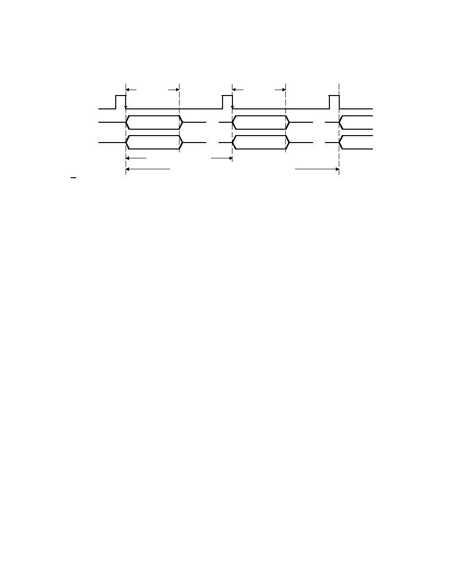
Figure 2–1. Timing Sequence of ADC Channel (Primary Communication Only)
FS
DOUT
(16-bit)
DOUT
(15+1-bit)
Primary
Secondary
16 SCLKs
# SCLKs Per Sampling Period (See Note C)
16–bit ADC Data
15–bit ADC Data + M/S
M/S+ Register Data/
M/S+ All 0 (See Note A)
# SCLKs (See Note B)
M/S+ Register Data/
M/S+ All 0 (See Note A)
Primary
16 SCLKs
NOTES: A. M/S bit (D15) in the secondary communication is used to indicate whether the register data (address and content) come from a
master device or a slave device if read bit is set. Otherwise, it is all 0s except M/S bit (master: M/S=1, slave: M/S=0).
B. The number of SCLKs between FS (primary) and FS (secondary) is 128 if cascading devices are less than 5, or 256 if cascading
devices are greater than 4.
C. The number of SCLKs per data sampling period is 256 if cascading devices are less than 5, or 512 if cascading devices are greater
than 4.
Figure 2–2. Timing Sequence of ADC Channel (Primary and Secondary Communication)
2.1.3
DAC Signal Channel
DIN received the 16-bit serial data word (2s complement) from the host during the primary communication interval.
These 16-bit digital words, representing analog output signal before PGA, are clocked into the serial port (DIN) at
the falling edge of SCLK during the frame-sync interval, one bit for each SCLK and one word for each primary
communication interval. The data are converted to a pulse train by the sigma-delta DAC comprised of a
digital-interpolation filter and a digital 1-bit modulator. The output of the modulator is then passed to an internal
low-pass filter to complete the signal reconstruction. Finally, the resulting analog signal is applied to the input of a
programmable-gain amplifier is capable of differentially driving a 600-ohm load at OUTP and OUTM. The timing
sequence is shown in Figure 2–3.
During secondary communication, the digital control and configuration data, together with the register address, are
clocked in through DIN (see Appendix A for register map). These 16-bit data are used either to initialize the register
or read out register content through DOUT. If a register initialization is not required, a no-operation word (D15-D9 are
all set to 0) can be used. If D12 is set to 1, the content of the control register, specified by D7-D0, will be sent out
through DOUT during the same secondary communication (see section 2.1.5). The timing sequence is shown in
Figure 2–4.
The interpolation FIR filter can be bypassed by writing a 1 to bit D1 of control register 1. The whole DAC channel can
be turned off for power savings by writing 10 to bits D2 and D1 of control register 3.
相关PDF资料 |
PDF描述 |
|---|---|
| TLV320AIC11IPFB | SPECIALTY CONSUMER CIRCUIT, PQFP48 |
| TLV320AIC11CPFBG4 | SPECIALTY CONSUMER CIRCUIT, PQFP48 |
| TLV320A11IPFBG4 | SPECIALTY CONSUMER CIRCUIT, PQFP48 |
| TLV320AIC11IPFBG4 | SPECIALTY CONSUMER CIRCUIT, PQFP48 |
| TLV320AIC13C | SPECIALTY CONSUMER CIRCUIT, PDSO30 |
相关代理商/技术参数 |
参数描述 |
|---|---|
| TLV320AIC11CPFBG4 | 功能描述:接口—CODEC 16-BIT D-TYPE LATCH RoHS:否 制造商:Texas Instruments 类型: 分辨率: 转换速率:48 kSPs 接口类型:I2C ADC 数量:2 DAC 数量:4 工作电源电压:1.8 V, 2.1 V, 2.3 V to 5.5 V 最大工作温度:+ 85 C 安装风格:SMD/SMT 封装 / 箱体:DSBGA-81 封装:Reel |
| TLV320AIC11EVM | 功能描述:音频 IC 开发工具 TLV320AIC11 Eval Mod RoHS:否 制造商:Texas Instruments 产品:Evaluation Kits 类型:Audio Amplifiers 工具用于评估:TAS5614L 工作电源电压:12 V to 38 V |
| TLV320AIC11I | 制造商:TI 制造商全称:Texas Instruments 功能描述:General-Purpose Low-Voltage 1.1V to 3.6V/0 16-bit 22-KSPS DSP CODEC |
| TLV320AIC11IPFB | 功能描述:接口—CODEC Gen Purp Lo-I/O Vltg 16-Bit 22-KSPS DSP RoHS:否 制造商:Texas Instruments 类型: 分辨率: 转换速率:48 kSPs 接口类型:I2C ADC 数量:2 DAC 数量:4 工作电源电压:1.8 V, 2.1 V, 2.3 V to 5.5 V 最大工作温度:+ 85 C 安装风格:SMD/SMT 封装 / 箱体:DSBGA-81 封装:Reel |
| TLV320AIC11IPFBG4 | 功能描述:接口—CODEC 12-Bit To 24-Bit Reg Bus Exchg W/3-St Otp RoHS:否 制造商:Texas Instruments 类型: 分辨率: 转换速率:48 kSPs 接口类型:I2C ADC 数量:2 DAC 数量:4 工作电源电压:1.8 V, 2.1 V, 2.3 V to 5.5 V 最大工作温度:+ 85 C 安装风格:SMD/SMT 封装 / 箱体:DSBGA-81 封装:Reel |
发布紧急采购,3分钟左右您将得到回复。