- 您现在的位置:买卖IC网 > PDF目录98252 > TLV320AIC11IPFBG4 (TEXAS INSTRUMENTS INC) SPECIALTY CONSUMER CIRCUIT, PQFP48 PDF资料下载
参数资料
| 型号: | TLV320AIC11IPFBG4 |
| 厂商: | TEXAS INSTRUMENTS INC |
| 元件分类: | 消费家电 |
| 英文描述: | SPECIALTY CONSUMER CIRCUIT, PQFP48 |
| 封装: | GREEN, PLASTIC, TQFP-48 |
| 文件页数: | 3/55页 |
| 文件大小: | 270K |
| 代理商: | TLV320AIC11IPFBG4 |
第1页第2页当前第3页第4页第5页第6页第7页第8页第9页第10页第11页第12页第13页第14页第15页第16页第17页第18页第19页第20页第21页第22页第23页第24页第25页第26页第27页第28页第29页第30页第31页第32页第33页第34页第35页第36页第37页第38页第39页第40页第41页第42页第43页第44页第45页第46页第47页第48页第49页第50页第51页第52页第53页第54页第55页
1–5
1.5
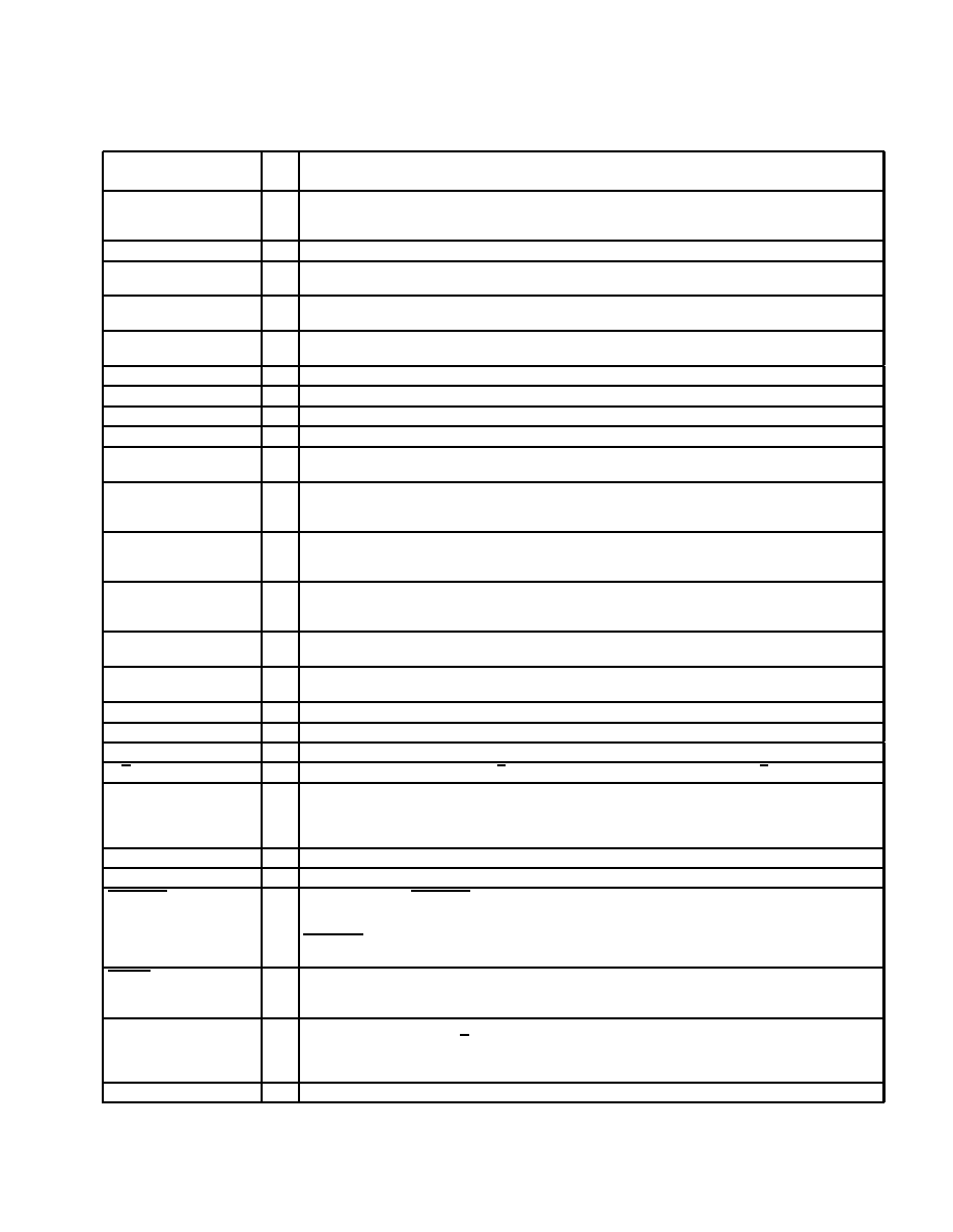
Terminal Functions (Continued)
TERMINAL
I/O
DESCRIPTION
NAME
NO.
I/O
DESCRIPTION
DOUT
16
O
Data output. DOUT transmits the ADC output bits and registers data, and is synchronized to SCLK and FS.
Data is sent out at the rising edge of SCLK when FS is low. DOUT is at high impedance when FS is not
activated.
DTXIM
7
I
Transmitter-path amplifier A3 analog inverting input. It can also be used for general-purpose amplification.
DTXIP
6
I
Transmitter-path amplifier A4 analog noninverting input. Can also be used for general-purpose
amplification.
DTXOM
5
O
Transmitter path amplifier A4 feedback for negative output. It can also be used for general-purpose
amplification.
DTXOP
4
O
Transmitter-path amplifier A3 feedback for positive output. It can also be used for general-purpose
amplification.
DVDD1
15
I
Dedicated 1.1-V to 3.6-V digital power supply for low-voltage I/O
DVDD2
30
I
Dedicated 3-V to 5.5-V digital power supply for core CODEC
DVSS
14, 29
I
Digital ground
FC
24
I
Hardware request for secondary communication
FILT
38
O
Bandgap filter. FILT is provided for decoupling of the bandgap reference, and provides 2.5 V. The optimal
capacitor value is 0.1
F (ceramic). This voltage node should be loaded only with a high-impedance dc load.
FLAG
23
O
Controlled by bit D4 of control register 3. If D4=0 (default), the FLAG pin outputs the communication flag that
goes low/high to indicate primary-communication/secondary-communication interval, respectively. If D4=1,
the FLAG pin outputs the value of D3.
FS
22
I/O
Frame sync. When FS goes low, DIN begins receiving data bits and DOUT begins transmitting data bits. In
master mode, FS is internally generated and is low during data transmission to DIN and from DOUT. In slave
mode, FS is externally generated.
FSD
21
O
Frame-sync delayed output. The FSD output synchronizes a slave device to the frame sync of the master
device. FSD is applied to the slave FS input and has the same duration as the master FS signal. Requires a
pullup resistor if not used.
INM
48
I
Inverting input to analog modulator. INM requires an external R-C antialias filter with low output impedance if
the internal antialias filter is bypassed.
INP
47
I
Noninverting input to analog modulator. INP requires an external R-C antialias filter with low output
impedance if the internal antialias filter is bypassed.
M0
10
I
Combine with M1 to select serial interface mode (frame-sync mode)
M1
11
I
Combine with M0 to select serial interface mode (frame-sync mode)
MCLK
20
I
Master clock. MCLK derives the internal clocks of the sigma-delta analog interface circuit.
M/S
27
I
Master/slave select input. When M/S is high, the device is the master, and when M/S is low, it is a slave.
NC
18, 28, 31,
32, 35, 36,
37, 39, 41,
44
No connection
OUTM
9
O
DAC’s inverting output. OUTM is functionally identical with and complementary to OUTP.
OUTP
8
O
DAC’s noninverting output. OUTP can also be used alone for single-ended operation.
PWRDWN
12
I
Power down. When PWRDWN is pulled low, the device goes into a power-down mode, the serial interface is
disabled, and most of the high-speed clocks are disabled. However, all register values are sustained and the
device resumes full-power operation without reinitialization when PWRDWN is pulled high again.
PWRDWN resets the counters only and preserves the programmed register contents. See paragraph 2.2.2
for more information.
RESET
13
I
Reset. The reset function is provided to initialize all the internal registers to their default values. The serial
port can be configured to the default state accordingly. See Appendix A, Register Set, and Subsection 2.2.1,
Reset and Power-Down Functions for detailed descriptions.
SCLK
19
I/O
Shift clock. SCLK signal clocks serial data into DIN and out of DOUT during the frame-sync interval. When
configured as an output (M/S high), SCLK is generated internally by multiplying the frame-sync signal
frequency by 256 (cascade devices < 5) or 512 (cascade devices > 4). When configured as an input (M/S
low), SCLK is generated externally and must be synchronous with the master clock and frame sync.
VMID
43
O
Reference voltage output at AVDD/2
相关PDF资料 |
PDF描述 |
|---|---|
| TLV320AIC13C | SPECIALTY CONSUMER CIRCUIT, PDSO30 |
| TLV320AIC13I | SPECIALTY CONSUMER CIRCUIT, PDSO30 |
| TLV320AIC14C | SPECIALTY CONSUMER CIRCUIT, PDSO30 |
| TLV320AIC14I | SPECIALTY CONSUMER CIRCUIT, PDSO30 |
| TLV320AIC22PT | SPECIALTY CONSUMER CIRCUIT, PQFP48 |
相关代理商/技术参数 |
参数描述 |
|---|---|
| TLV320AIC11PFB | 制造商:TI 制造商全称:Texas Instruments 功能描述:General-Purpose Low-Voltage 1.1V to 3.6V/0 16-bit 22-KSPS DSP CODEC |
| TLV320AIC12 | 制造商:TI 制造商全称:Texas Instruments 功能描述:PRODUCT NOTIFICATION |
| TLV320AIC12_07 | 制造商:TI 制造商全称:Texas Instruments 功能描述:LOW-POWER, HIGHLY-INTEGRATED, PROGRAMMABLE 16-Bit, 26-KSPS MONO CODEC |
| TLV320AIC12CDBT | 功能描述:接口—CODEC Lo-Pwr Mono Voice Band CODEC RoHS:否 制造商:Texas Instruments 类型: 分辨率: 转换速率:48 kSPs 接口类型:I2C ADC 数量:2 DAC 数量:4 工作电源电压:1.8 V, 2.1 V, 2.3 V to 5.5 V 最大工作温度:+ 85 C 安装风格:SMD/SMT 封装 / 箱体:DSBGA-81 封装:Reel |
| TLV320AIC12CDBTG4 | 功能描述:接口—CODEC Lo-Pwr Mono Voice Band CODEC RoHS:否 制造商:Texas Instruments 类型: 分辨率: 转换速率:48 kSPs 接口类型:I2C ADC 数量:2 DAC 数量:4 工作电源电压:1.8 V, 2.1 V, 2.3 V to 5.5 V 最大工作温度:+ 85 C 安装风格:SMD/SMT 封装 / 箱体:DSBGA-81 封装:Reel |
发布紧急采购,3分钟左右您将得到回复。