参数资料
| 型号: | TLV342SIRUGRG4 |
| 厂商: | Texas Instruments |
| 文件页数: | 31/36页 |
| 文件大小: | 0K |
| 描述: | IC OPAMP GP R-R 2.3MHZ 10QFN |
| 标准包装: | 3,000 |
| 放大器类型: | 通用 |
| 电路数: | 2 |
| 输出类型: | 满摆幅 |
| 转换速率: | 1 V/µs |
| 增益带宽积: | 2.3MHz |
| 电流 - 输入偏压: | 1pA |
| 电压 - 输入偏移: | 300µV |
| 电流 - 电源: | 75µA |
| 电流 - 输出 / 通道: | 115mA |
| 电压 - 电源,单路/双路(±): | 1.5 V ~ 5.5 V |
| 工作温度: | -40°C ~ 125°C |
| 安装类型: | 表面贴装 |
| 封装/外壳: | 10-XFQFN |
| 供应商设备封装: | 10-X2QFN-EP(2x1.5) |
| 包装: | 带卷 (TR) |
第1页第2页第3页第4页第5页第6页第7页第8页第9页第10页第11页第12页第13页第14页第15页第16页第17页第18页第19页第20页第21页第22页第23页第24页第25页第26页第27页第28页第29页第30页当前第31页第32页第33页第34页第35页第36页
TLV341, TLV342, TLV342S, TLV344
LOW-VOLTAGE RAIL-TO-RAIL OUTPUT CMOS OPERATIONAL AMPLIFIERS
WITH SHUTDOWN
SLVS568C JANUARY 2005 REVISED NOVEMBER 2007
4
POST OFFICE BOX 655303
DALLAS, TEXAS 75265
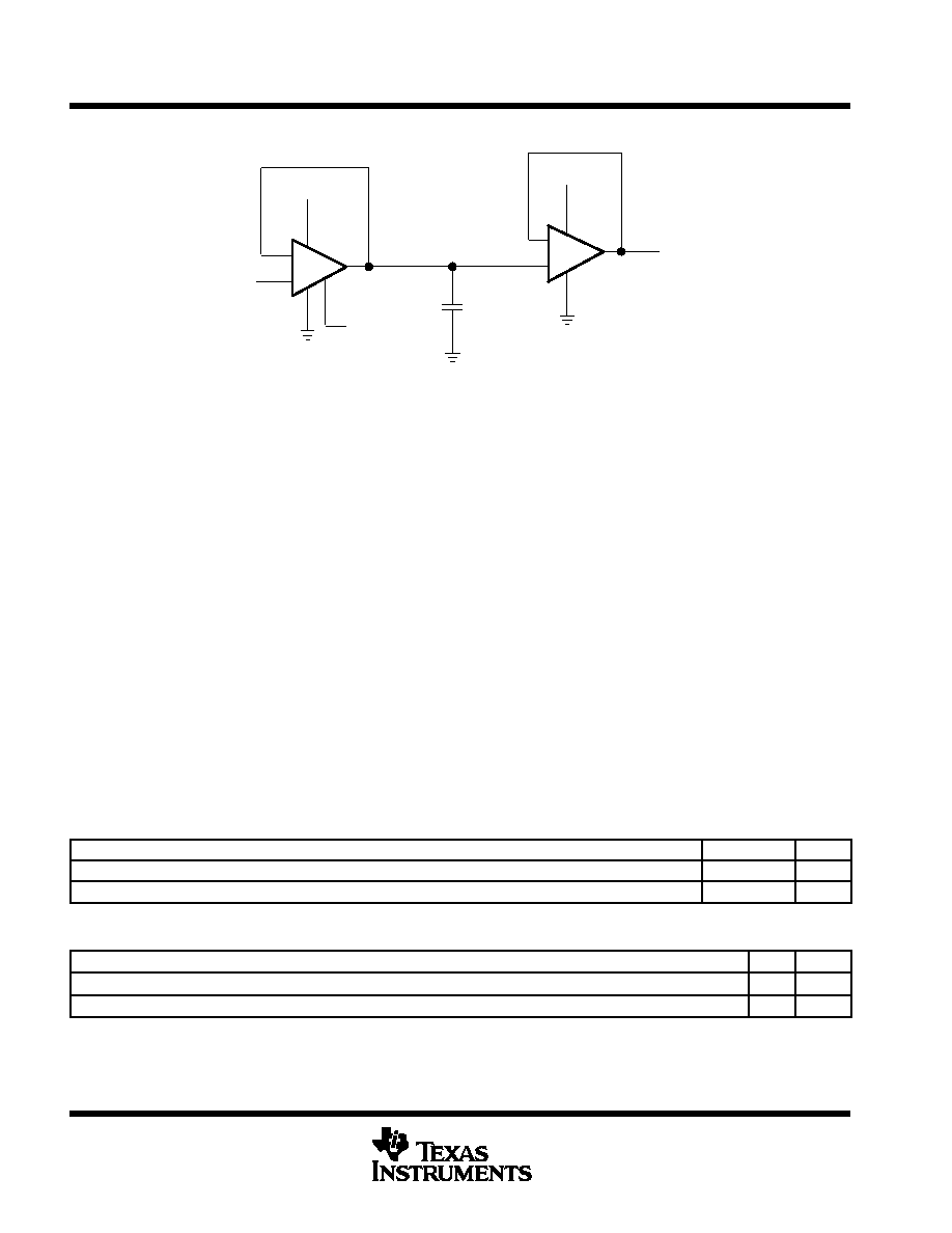
symbol (each amplifier)
V+
VO
+
VI
+
C = 200 pF
V+
Sample
Clock
absolute maximum ratings over operating free-air temperature range (unless otherwise noted)
Supply voltage, V+ (see Note 1)
5.5 V
. . . . . . . . . . . . . . . . . . . . . . . . . . . . . . . . . . . . . . . . . . . . . . . . . . . . . . . . . . . . .
Differential input voltage, VID (see Note 2)
±5.5 V
. . . . . . . . . . . . . . . . . . . . . . . . . . . . . . . . . . . . . . . . . . . . . . . . . . .
Input voltage range, VI (either input)
0 to 5.5 V
. . . . . . . . . . . . . . . . . . . . . . . . . . . . . . . . . . . . . . . . . . . . . . . . . . . . .
Package thermal impedance,
θJA (see Notes 3 and 4): D package (8 pin)
97
°C/W
. . . . . . . . . . . . . . . . . . . . . .
D package (14 pin)
86
°C/W
. . . . . . . . . . . . . . . . . . . . .
DBV package
165
°C/W
. . . . . . . . . . . . . . . . . . . . . . . .
DCK package
259
°C/W
. . . . . . . . . . . . . . . . . . . . . . . .
DGK package
172
°C/W
. . . . . . . . . . . . . . . . . . . . . . . .
DRL package
142
°C/W
. . . . . . . . . . . . . . . . . . . . . . . .
PW package
113
°C/W
. . . . . . . . . . . . . . . . . . . . . . . . .
RUG package
243
°C/W
. . . . . . . . . . . . . . . . . . . . . . . .
Operating virtual junction temperature
150
°C
. . . . . . . . . . . . . . . . . . . . . . . . . . . . . . . . . . . . . . . . . . . . . . . . . . . . . .
Storage temperature range, Tstg
65
°C to 150°C
. . . . . . . . . . . . . . . . . . . . . . . . . . . . . . . . . . . . . . . . . . . . . . . . . . .
Stresses beyond those listed under “absolute maximum ratings” may cause permanent damage to the device. These are stress ratings only, and
functional operation of the device at these or any other conditions beyond those indicated under “recommended operating conditions” is not
implied. Exposure to absolute-maximum-rated conditions for extended periods may affect device reliability.
NOTES:
1. All voltage values (except differential voltages and V+ specified for the measurement of IOS) are with respect to the network GND.
2. Differential voltages are at IN+ with respect to IN.
3. Maximum power dissipation is a function of TJ(max),
θJA, and TA. The maximum allowable power dissipation at any allowable
ambient temperature is PD = (TJ(max) TA)/
θJA. Selecting the maximum of 150°C can affect reliability.
4. The package thermal impedance is calculated in accordance with JESD 51-7.
recommended operating conditions
MIN
MAX
UNIT
V+
Supply voltage (single-supply operation)
1.5
5.5
V
TA
Operating free-air temperature
40
125
°C
ESD protection
TEST CONDITIONS
TYP
UNIT
Human-Body Model
2000
V
Machine Model
200
V
相关PDF资料 |
PDF描述 |
|---|---|
| TLV342IRUGRG4 | IC OPAMP GP R-R 2.3MHZ 10QFN |
| GTCA28-102M-P03 | GAS TUBE 8MM 1000V 20% 3KA AXIAL |
| TLV342IDGKRG4 | IC OPAMP GP R-R 2.3MHZ 8MSOP |
| GTCA26-351M-P05 | GAS TUBE 6MM 350V 20% 5KA AXIAL |
| TLV341AIDCKRG4 | IC OPAMP GP R-R 2.3MHZ SC70-6 |
相关代理商/技术参数 |
参数描述 |
|---|---|
| TLV344 | 制造商:TI 制造商全称:Texas Instruments 功能描述:LOW-VOLTAGE RAIL-TO-RAIT OUTPUT CMOS OPERATIONAL AMPLIFIERS |
| TLV344AID | 制造商:TI 制造商全称:Texas Instruments 功能描述:LOW-VOLTAGE RAIL-TO-RAIL OUTPUT CMOS OPERATIONAL AMPLIFIERS WITH SHUTDOWN |
| TLV344AIDR | 制造商:TI 制造商全称:Texas Instruments 功能描述:LOW-VOLTAGE RAIL-TO-RAIL OUTPUT CMOS OPERATIONAL AMPLIFIERS WITH SHUTDOWN |
| TLV344AIPWR | 制造商:TI 制造商全称:Texas Instruments 功能描述:LOW-VOLTAGE RAIL-TO-RAIL OUTPUT CMOS OPERATIONAL AMPLIFIERS WITH SHUTDOWN |
| TLV344D | 制造商:TI 制造商全称:Texas Instruments 功能描述:LOW-VOLTAGE RAIL-TO-RAIL OUTPUT CMOS OPERATIONAL AMPLIFIERS WITH SHUTDOWN |
发布紧急采购,3分钟左右您将得到回复。