- 您现在的位置:买卖IC网 > PDF目录98255 > TLV5580CPWR (TEXAS INSTRUMENTS INC) 1-CH 8-BIT PROPRIETARY METHOD ADC, PARALLEL ACCESS, PDSO28 PDF资料下载
参数资料
| 型号: | TLV5580CPWR |
| 厂商: | TEXAS INSTRUMENTS INC |
| 元件分类: | ADC |
| 英文描述: | 1-CH 8-BIT PROPRIETARY METHOD ADC, PARALLEL ACCESS, PDSO28 |
| 封装: | GREEN, PLASTIC, TSSOP-28 |
| 文件页数: | 13/36页 |
| 文件大小: | 478K |
| 代理商: | TLV5580CPWR |
第1页第2页第3页第4页第5页第6页第7页第8页第9页第10页第11页第12页当前第13页第14页第15页第16页第17页第18页第19页第20页第21页第22页第23页第24页第25页第26页第27页第28页第29页第30页第31页第32页第33页第34页第35页第36页
TLV5580
8BIT, 80 MSPS LOW POWER A/D CONVERTER
SLAS205B DECEMBER 1998 REVISED OCTOBER 2003
www.ti.com
20
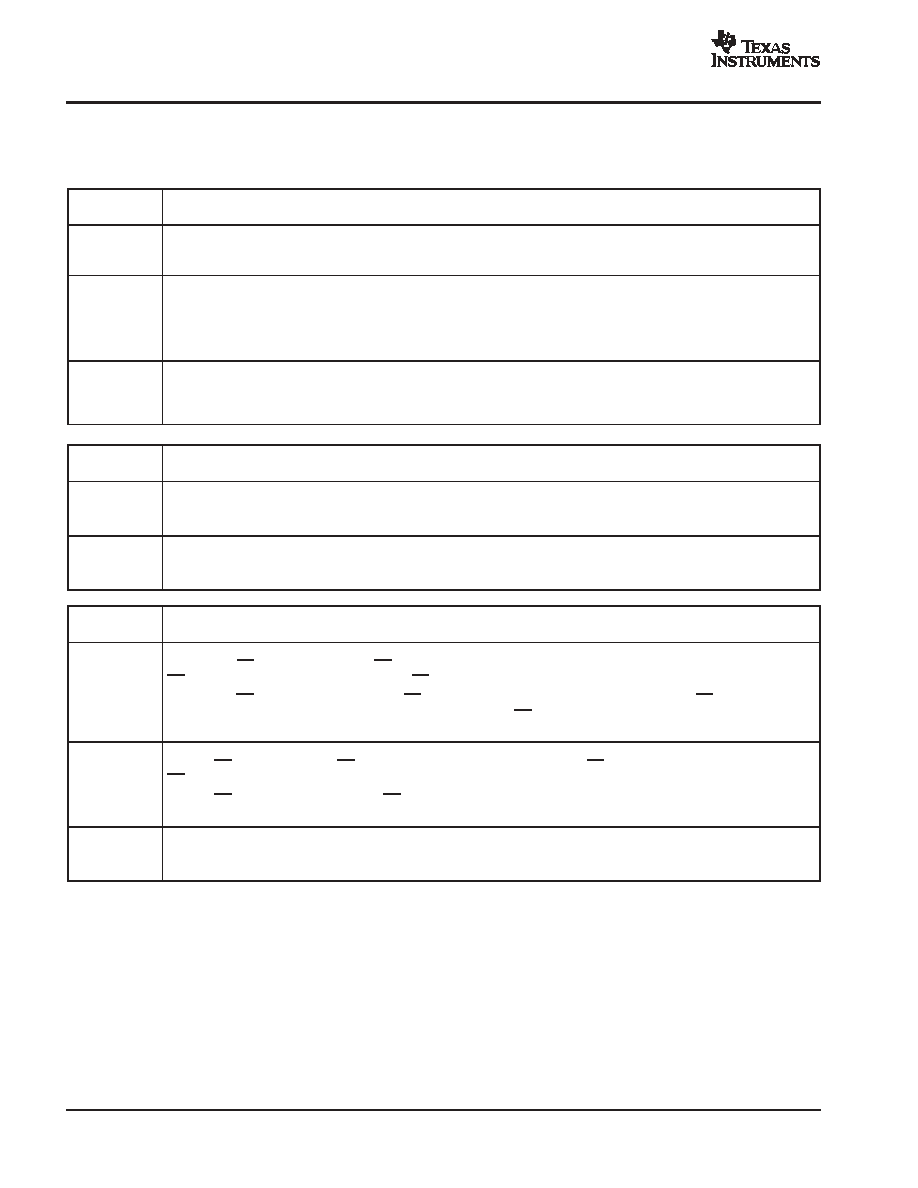
TLV5580 EVALUATION MODULE
TLV5580 EVM SETTINGS
CLOCK INPUT SETTINGS
REFERENCE
DESIGNATOR
FUNCTION
W1
Clock selection switch
12 J11: clock from pin1 on J11 connector
23 J9: clock from J9 SMA connector
W2
Clock source switch
J XTL: clock from onboard crystal oscillator
j CLK: clock from pin 1 on J11 connector (if W1/12) or J9 SMA connector (if W1/23)
NOTE: If set to XTL and a XTL oscillator is populated, no clock signal should be applied to J9 or J11, depending on the W1
setting.
W3
Clock output switch
12 Rising: clock output on J11 connector is the same phase as the clock to the digital output buffer. Data changes on rising
CLK edge.
23 Falling: clock output on J11 connector is the opposite phase as the digital output buffer. Data changes on falling CLK edge.
REFERENCE SETTINGS
REFERENCE
DESIGNATOR
FUNCTION
SW1
REFT external/internal switch
Jj REFT internal: REFT from TLV5580 internal reference
jJ REFT external: REFT from onboard voltage reference circuit
SW2
REFB external/internal switch
Jj REFB internal: REFB from TLV5580 internal reference
jJ REFB external: REFB from onboard voltage reference circuit
CONTROL SETTINGS
REFERENCE
DESIGNATOR
FUNCTION
W4
TLV5580 and digital output buffer output enable control (1)
J 5580-574 OE-connected: Connects OEs of TLV5580 and digital output buffer (574 buffer). Use this when no board-external
OE is used. In addition, close W5 to have both OEs permanently enabled.
j 5580-574OE-disconnected: Disconnects OEs of TLV5580 and digital output buffer (574 buffer). The OE for the output buffer
needs to be pulled low from pin 5 on J11 connector to enable. The OE for TLV5580 is independently controlled from pin 7 on
J11 connector (W5 open) or is permanently enabled if W5 is closed.
W5
TLV5580 and digital output buffer output enable control (2)
J 5580 OE to GND: Connects OEs of TLV5580 to GND. Additionally connects OE of 74ALS574 to GND if W4 is 5580-574
OE-connected.
j 5580 OE external: Enables control of OE of TLV5580 via pin 7 on J11 connector. When taken high (internal pulldown) the
output can be disabled.
W6
TLV5580 STDBY control
J Stdby: STDBY is active (high).
j Active: STDBY is low, via internal pulldown. STDBY can be taken high from pin 9 on J11 connector to enable standby mode.
相关PDF资料 |
PDF描述 |
|---|---|
| TLV5580IPWG4 | 1-CH 8-BIT PROPRIETARY METHOD ADC, PARALLEL ACCESS, PDSO28 |
| TLV5580CPWRG4 | 1-CH 8-BIT PROPRIETARY METHOD ADC, PARALLEL ACCESS, PDSO28 |
| TLV5580IPWRG4 | 1-CH 8-BIT PROPRIETARY METHOD ADC, PARALLEL ACCESS, PDSO28 |
| TLV5580IDWR | 1-CH 8-BIT PROPRIETARY METHOD ADC, PARALLEL ACCESS, PDSO28 |
| TLV5580IPW | 1-CH 8-BIT PROPRIETARY METHOD ADC, PARALLEL ACCESS, PDSO28 |
相关代理商/技术参数 |
参数描述 |
|---|---|
| TLV5580CPWRG4 | 功能描述:模数转换器 - ADC 8Bit 80MSPS 1-Ch High Ch Band Lo-Pwr RoHS:否 制造商:Texas Instruments 通道数量:2 结构:Sigma-Delta 转换速率:125 SPs to 8 KSPs 分辨率:24 bit 输入类型:Differential 信噪比:107 dB 接口类型:SPI 工作电源电压:1.7 V to 3.6 V, 2.7 V to 5.25 V 最大工作温度:+ 85 C 安装风格:SMD/SMT 封装 / 箱体:VQFN-32 |
| TLV5580DW | 制造商:TI 制造商全称:Texas Instruments 功能描述:8-BIT, 80 MSPS LOW-POWER A/D CONVERTER |
| TLV5580EVM | 制造商:Texas Instruments 功能描述:EVAL BD FOR TLV5580 8BIT 80 MSPS HIGH-SPEED A/D CNVRTR - Bulk |
| TLV5580IDW | 功能描述:模数转换器 - ADC _ RoHS:否 制造商:Texas Instruments 通道数量:2 结构:Sigma-Delta 转换速率:125 SPs to 8 KSPs 分辨率:24 bit 输入类型:Differential 信噪比:107 dB 接口类型:SPI 工作电源电压:1.7 V to 3.6 V, 2.7 V to 5.25 V 最大工作温度:+ 85 C 安装风格:SMD/SMT 封装 / 箱体:VQFN-32 |
| TLV5580IDWG4 | 功能描述:模数转换器 - ADC 8Bit 80MSPS 1-Ch High Ch Band Lo-Pwr RoHS:否 制造商:Texas Instruments 通道数量:2 结构:Sigma-Delta 转换速率:125 SPs to 8 KSPs 分辨率:24 bit 输入类型:Differential 信噪比:107 dB 接口类型:SPI 工作电源电压:1.7 V to 3.6 V, 2.7 V to 5.25 V 最大工作温度:+ 85 C 安装风格:SMD/SMT 封装 / 箱体:VQFN-32 |
发布紧急采购,3分钟左右您将得到回复。