- 您现在的位置:买卖IC网 > PDF目录98256 > TLV5580IPW (TEXAS INSTRUMENTS INC) 1-CH 8-BIT PROPRIETARY METHOD ADC, PARALLEL ACCESS, PDSO28 PDF资料下载
参数资料
| 型号: | TLV5580IPW |
| 厂商: | TEXAS INSTRUMENTS INC |
| 元件分类: | ADC |
| 英文描述: | 1-CH 8-BIT PROPRIETARY METHOD ADC, PARALLEL ACCESS, PDSO28 |
| 封装: | GREEN, PLASTIC, TSSOP-28 |
| 文件页数: | 36/36页 |
| 文件大小: | 478K |
| 代理商: | TLV5580IPW |
第1页第2页第3页第4页第5页第6页第7页第8页第9页第10页第11页第12页第13页第14页第15页第16页第17页第18页第19页第20页第21页第22页第23页第24页第25页第26页第27页第28页第29页第30页第31页第32页第33页第34页第35页当前第36页
TLV5580
8BIT, 80 MSPS LOW POWER A/D CONVERTER
SLAS205B DECEMBER 1998 REVISED OCTOBER 2003
www.ti.com
9
ELECTRICAL CHARACTERISTICS OVER RECOMMENDED OPERATING CONDITIONS WITH FCLK = 80
MSPS AND USE OF EXTERNAL VOLTAGE REFERENCES (unless otherwise noted) (continued)
TIMING REQUIREMENTS
PARAMETER
TEST CONDITIONS
MIN
TYP
MAX
UNIT
fclk
Maximum conversion rate
80
MHz
fclk
Minimum conversion rate
10
kHz
td(o)
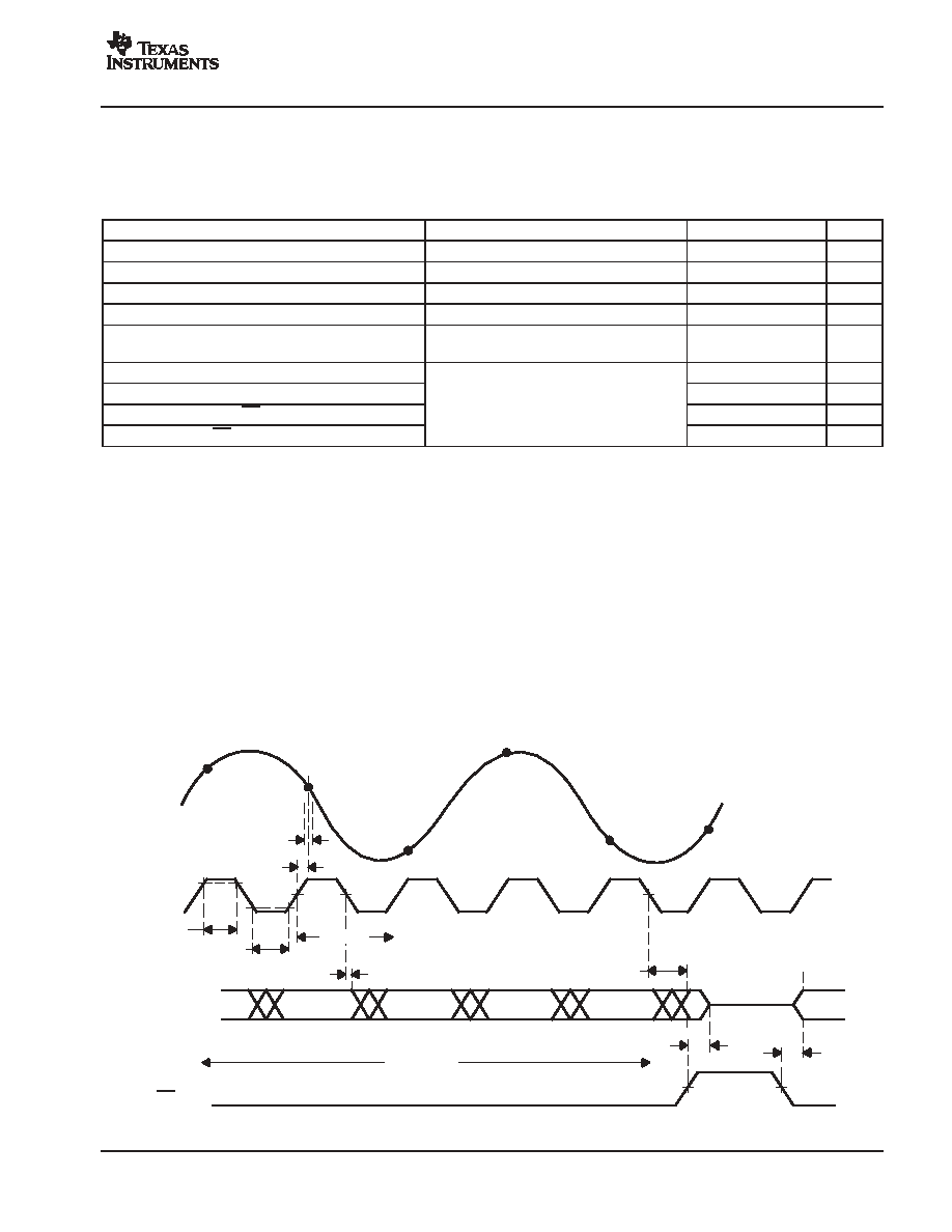
Output delay time (see Figure 1)
CL = 10 pF,
See Notes 5 and 6
4.5
9
ns
th(o)
Output hold time
CL = 2 pF,
See Note 5
2
ns
td(pipe)
Pipeline delay (latency)
See Note 6
4.5
CLK
cycles
td(a)
Aperture delay time
3
ns
tj(a)
Aperture jitter
See Note 5
1.5
ps, rms
tdis
Disable time, OE rising to Hi-Z
See Note 5
5
8
ns
ten
Enable, OE falling to valid data
5
8
ns
5. Output timing td(o) is measured from the 1.5 V level of the CLK input falling edge to the 10%/90% level of the digital output. The digital output load
is not higher than 10 pF.
Output hold time th(o) is measured from the 1.5 V level of the CLK input falling edge to the 10%/90% level of the digital output. The digital output
is load is not less than 2 pF.
Aperture delay td(A) is measured from the 1.5 V level of the CLK input to the actual sampling instant.
The OE signal is asynchronous.
OE timing tdis is measured from the VIH(MIN) level of OE to the high-impedance state of the output data. The digital output load is not higher than
10 pF.
OE timing ten is measured from the VIL(MAX) level of OE to the instant when the output data reaches VOH(min) or VOL(max) output levels. The digital
output load is not higher than 10 pF.
6. The number of clock cycles between conversion initiation on an input sample and the corresponding output data being made available from the
ADC pipeline. Once the data pipeline is full, new valid output data is provided on every clock cycle. In order to know when data is stable on the
output pins, the output delay time td(o) (i.e., the delay time through the digital output buffers) needs to be added to the pipeline latency. Note that
since the max. td(o) is more than 1/2 clock period at 80 MHz; data cannot be reliably clocked in on a rising edge of CLK at this speed. The falling
edge should be used.
D0D7
N4
N3
N2
N1
N
N+1
N
N+1
N+2
N+3
N+4
N+5
tj(A)
td(A)
VIL
(max)
1.5 V
tw(CLKH)
tw(CLKL)
1/fCLK
th(o)
1.5 V
td(o)
tdis
ten
CLK
OE
90%
10%
VIH(min)
td(pipe)
VOH(min)
VOL(max)
VIL(max)
VIH
(min)
Figure 1. Timing Diagram
相关PDF资料 |
PDF描述 |
|---|---|
| TLV5580IPWR | 1-CH 8-BIT PROPRIETARY METHOD ADC, PARALLEL ACCESS, PDSO28 |
| TLV5580IDWG4 | 1-CH 8-BIT PROPRIETARY METHOD ADC, PARALLEL ACCESS, PDSO28 |
| TLV5580CDWG4 | 1-CH 8-BIT PROPRIETARY METHOD ADC, PARALLEL ACCESS, PDSO28 |
| TLV5580CPWG4 | 1-CH 8-BIT PROPRIETARY METHOD ADC, PARALLEL ACCESS, PDSO28 |
| TLV5590ED | 1-CH 2-BIT PROPRIETARY METHOD ADC, PARALLEL ACCESS, PDSO14 |
相关代理商/技术参数 |
参数描述 |
|---|---|
| TLV5580IPWG4 | 功能描述:模数转换器 - ADC 8B 80MSPS ADC Sgl Ch Hi Ch BW Lo Pwr RoHS:否 制造商:Texas Instruments 通道数量:2 结构:Sigma-Delta 转换速率:125 SPs to 8 KSPs 分辨率:24 bit 输入类型:Differential 信噪比:107 dB 接口类型:SPI 工作电源电压:1.7 V to 3.6 V, 2.7 V to 5.25 V 最大工作温度:+ 85 C 安装风格:SMD/SMT 封装 / 箱体:VQFN-32 |
| TLV5580IPWR | 功能描述:模数转换器 - ADC 8Bit 80MSPS 1-Ch High Ch Band Lo-Pwr RoHS:否 制造商:Texas Instruments 通道数量:2 结构:Sigma-Delta 转换速率:125 SPs to 8 KSPs 分辨率:24 bit 输入类型:Differential 信噪比:107 dB 接口类型:SPI 工作电源电压:1.7 V to 3.6 V, 2.7 V to 5.25 V 最大工作温度:+ 85 C 安装风格:SMD/SMT 封装 / 箱体:VQFN-32 |
| TLV5580IPWRG4 | 功能描述:模数转换器 - ADC 8Bit 80MSPS 1-Ch High Ch Band Lo-Pwr RoHS:否 制造商:Texas Instruments 通道数量:2 结构:Sigma-Delta 转换速率:125 SPs to 8 KSPs 分辨率:24 bit 输入类型:Differential 信噪比:107 dB 接口类型:SPI 工作电源电压:1.7 V to 3.6 V, 2.7 V to 5.25 V 最大工作温度:+ 85 C 安装风格:SMD/SMT 封装 / 箱体:VQFN-32 |
| TLV5580PW | 制造商:TI 制造商全称:Texas Instruments 功能描述:8-BIT, 80 MSPS LOW-POWER A/D CONVERTER |
| TLV5590 | 制造商:TI 制造商全称:Texas Instruments 功能描述:2-BIT ANALOG-TO-DIGITAL CONVERTER FOR FLEX |
发布紧急采购,3分钟左右您将得到回复。