- 您现在的位置:买卖IC网 > PDF目录98257 > TLV5610IYER (TEXAS INSTRUMENTS INC) SERIAL INPUT LOADING, 3 us SETTLING TIME, 12-BIT DAC, PBGA20 PDF资料下载
参数资料
| 型号: | TLV5610IYER |
| 厂商: | TEXAS INSTRUMENTS INC |
| 元件分类: | DAC |
| 英文描述: | SERIAL INPUT LOADING, 3 us SETTLING TIME, 12-BIT DAC, PBGA20 |
| 封装: | WAFER CHIP SCALE, 20 PIN |
| 文件页数: | 5/17页 |
| 文件大小: | 345K |
| 代理商: | TLV5610IYER |
TLV5610IYE
TLV5608IYE
SLAS393 OCTOBER 2003
www.ti.com
13
USING TLV5610IYE AND TLV5608IYE, WAFER CHIP SCALE PACKAGE (WCS)
D TLV5610 and TLV5608 qualifications were done using a wire-bonded small outline (SOIC) package and
includes: steady state life, thermal shock, ESD, latch-up, biased HAST, autoclave, and characterization.
These qualified devices are orderable as TLV5610IDW and TLV5608IDW.
D The wafer chip-scale package (WCS), TLV5610IYE and TLV5608IYE, uses the same DIE as
TLV5610IDW and TLV5608IDW respectively, but are not qualified. WCS qualification, including board
level reliability (BLR), is the responsibility of the customer.
D It is recommended that underfill be used for increased reliability. BLR is application dependent, but may
include test such as: temperature cycling, drop test, key push, bend, vibration, and package shear.
The following WCSP information provides the user of the TLV5610IYE and TLV5608IYE with some general
guidelines for board assembly.
D Melting point of eutectic solder is 183°C.
D Recommended peak reflow temperatures are in the 220°C to 230°C range.
D The use of underfill is required. The use of underfill greatly reduces the risk of thermal mismatch fails.
Underfill is an epoxy/adhesive that may be added during the board assembly process to improve board
level/system level reliability. The process is to dispense the epoxy under the dice after die attach reflow. The
epoxy adheres to the body of the device and to the printed-circuit board. It reduces stress placed upon the solder
joints due to the thermal coefficient of expansion (TCE) mismatch between the board and the component.
Underfill material is highly filled with silica or other fillers to increase an epoxy’s modulus, reduce creep
sensitivity, and decrease the material’s TCE.
The recommendation for peak flow temperatures of 220
°C to 230°C is based on general empirical results that
indicate that this temperature range is needed to facilitate good wetting of the solder bump to the substrate or
circuit board pad. Lower peak temperatures may cause nonwets (cold solder joints).
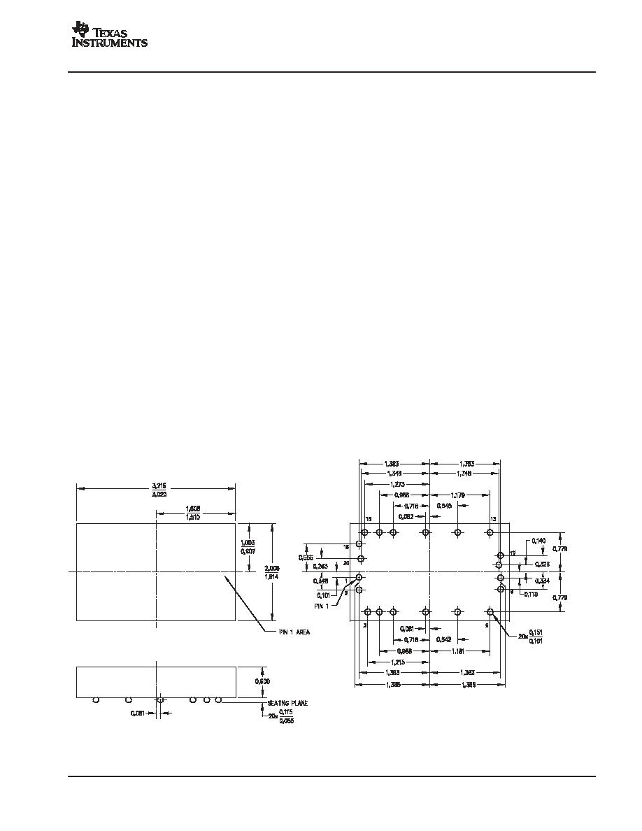
Bottom View
Top View
NOTES:A. All linear dimensions are in millimeters.
B. This drawing is subject to change without notice.
Figure 11. TLV5610IYE and TLV5608IYE Wafer Chip Scale Package
相关PDF资料 |
PDF描述 |
|---|---|
| TLV5610IYZT | SERIAL INPUT LOADING, 3 us SETTLING TIME, 12-BIT DAC, BGA20 |
| TLV5610IYZR | SERIAL INPUT LOADING, 3 us SETTLING TIME, 12-BIT DAC, BGA20 |
| TLV5610IYZ | SERIAL INPUT LOADING, 3 us SETTLING TIME, 12-BIT DAC, BGA20 |
| TLV5613CDWRG4 | PARALLEL, WORD INPUT LOADING, 1 us SETTLING TIME, 12-BIT DAC, PDSO20 |
| TLV5613IDW | PARALLEL, WORD INPUT LOADING, 1 us SETTLING TIME, 12-BIT DAC, PDSO20 |
相关代理商/技术参数 |
参数描述 |
|---|---|
| TLV5610IYZ | 制造商:TI 制造商全称:Texas Instruments 功能描述:DIGITAL-TO-ANALOG CONVERTER in a Wafer Chip-Scale Packagea??Pb-Free/Green |
| TLV5610IYZR | 功能描述:数模转换器- DAC 2.7V to 5.5V 12B Octal DAC RoHS:否 制造商:Texas Instruments 转换器数量:1 DAC 输出端数量:1 转换速率:2 MSPs 分辨率:16 bit 接口类型:QSPI, SPI, Serial (3-Wire, Microwire) 稳定时间:1 us 最大工作温度:+ 85 C 安装风格:SMD/SMT 封装 / 箱体:SOIC-14 封装:Tube |
| TLV5610IYZT | 功能描述:数模转换器- DAC 2.7V to 5.5V 12B Octal DAC RoHS:否 制造商:Texas Instruments 转换器数量:1 DAC 输出端数量:1 转换速率:2 MSPs 分辨率:16 bit 接口类型:QSPI, SPI, Serial (3-Wire, Microwire) 稳定时间:1 us 最大工作温度:+ 85 C 安装风格:SMD/SMT 封装 / 箱体:SOIC-14 封装:Tube |
| TLV5613 | 制造商:TI 制造商全称:Texas Instruments 功能描述:2.7 V TO 5.5 V 12-BIT PARALLEL DIGITAL-TO-ANALOG CONVERTER WITH POWER DOWN |
| TLV5613CDW | 功能描述:数模转换器- DAC 12bit CMOS DAC RoHS:否 制造商:Texas Instruments 转换器数量:1 DAC 输出端数量:1 转换速率:2 MSPs 分辨率:16 bit 接口类型:QSPI, SPI, Serial (3-Wire, Microwire) 稳定时间:1 us 最大工作温度:+ 85 C 安装风格:SMD/SMT 封装 / 箱体:SOIC-14 封装:Tube |
发布紧急采购,3分钟左右您将得到回复。