- 您现在的位置:买卖IC网 > PDF目录98262 > TLV62065DSGT (TEXAS INSTRUMENTS INC) 2 A SWITCHING REGULATOR, 3400 kHz SWITCHING FREQ-MAX, PDSO8 PDF资料下载
参数资料
| 型号: | TLV62065DSGT |
| 厂商: | TEXAS INSTRUMENTS INC |
| 元件分类: | 稳压器 |
| 英文描述: | 2 A SWITCHING REGULATOR, 3400 kHz SWITCHING FREQ-MAX, PDSO8 |
| 封装: | 2 X 2 MM, 0.75 MM HEIGHT, PLASTIC, WSON-8 |
| 文件页数: | 6/26页 |
| 文件大小: | 1182K |
| 代理商: | TLV62065DSGT |
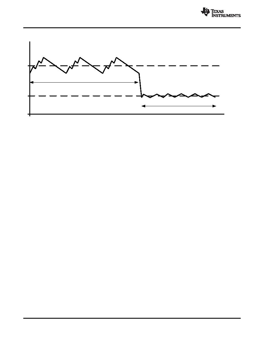
Outputvoltage
Vout (PWM)
Vout +1%
PFMComparator
threshold
VoltagePositioning
Lightload
PFMMode
moderatetoheavyload
PWMMode
SLVSAC4 – NOVEMBER 2010
www.ti.com
Figure 22. Power Save Mode Operation with automatic Mode transition
100% Duty Cycle Low Dropout Operation
The device starts to enter 100% duty cycle mode as the input voltage comes close to the nominal output voltage.
In order to maintain the output voltage, the High-Side MOSFET switch is turned on 100% for one or more cycles.
With further decreasing VIN the High-Side MOSFET switch is turned on completely. In this case the converter
offers a low input-to-output voltage difference. This is particularly useful in battery-powered applications to
achieve longest operation time by taking full advantage of the whole battery voltage range.
The minimum input voltage to maintain regulation depends on the load current and output voltage, and can be
calculated as:
VINmin = VOmax + IOmax × (RDS(on)max + RL)
With:
IOmax = maximum output current
RDS(on)max = maximum P-channel switch RDS(on).
RL = DC resistance of the inductor
VOmax = nominal output voltage plus maximum output voltage tolerance
Undervoltage Lockout
The under voltage lockout circuit prevents the device from malfunctioning at low input voltages and from
excessive discharge of the battery. It disables the output stage of the converter once the falling VIN trips the
under-voltage lockout threshold VUVLO. The under-voltage lockout threshold VUVLO for falling VIN is typically
1.78V. The device starts operation once the rising VIN trips under-voltage lockout threshold VUVLO again at
typically 1.95V.
Output Capacitor Discharge
With EN = GND, the device enters shutdown mode and all internal circuits are disabled. The SW pin is
connected to PGND via an internal resistor to discharge the output capacitor. This feature ensures a startup in a
discharged output capacitor once the converter is enabled again and prevents "floating" charge on the output
capacitor. The output voltage ramps up monotonic starting from 0V.
MODE SELECTION
The MODE pin allows mode selection between forced PWM mode and Power Save Mode.
14
Copyright 2010, Texas Instruments Incorporated
Product Folder Link(s) :TLV62065
相关PDF资料 |
PDF描述 |
|---|---|
| TLV977-10CPFB | SPECIALTY ANALOG CIRCUIT, PQFP48 |
| TLV987CPFB | SPECIALTY ANALOG CIRCUIT, PQFP48 |
| TLV990-13PFB | SPECIALTY CONSUMER CIRCUIT, PQFP48 |
| TLV990-13PFBG4 | SPECIALTY CONSUMER CIRCUIT, PQFP48 |
| TLV990-21PFB | SPECIALTY CONSUMER CIRCUIT, PQFP48 |
相关代理商/技术参数 |
参数描述 |
|---|---|
| TLV62065EVM719 | 制造商:Texas Instruments 功能描述:TLV62065EVM719 |
| TLV62065EVM-719 | 功能描述:电源管理IC开发工具 TLV62065 Eval Mod RoHS:否 制造商:Maxim Integrated 产品:Evaluation Kits 类型:Battery Management 工具用于评估:MAX17710GB 输入电压: 输出电压:1.8 V |
| TLV62065-Q1 | 制造商:TI 制造商全称:Texas Instruments 功能描述:3-MHz 2-A Step-Down Converter in 2-mm x 2-mm SON Package |
| TLV62065TDSGRQ1 | 功能描述:直流/直流开关转换器 AC 3MHz,2A SD Converter RoHS:否 制造商:STMicroelectronics 最大输入电压:4.5 V 开关频率:1.5 MHz 输出电压:4.6 V 输出电流:250 mA 输出端数量:2 最大工作温度:+ 85 C 安装风格:SMD/SMT |
| TLV62080 | 制造商:TI 制造商全称:Texas Instruments 功能描述:1.2A High Efficient Step Down Converter in 2x2mm SON Package |
发布紧急采购,3分钟左右您将得到回复。