- 您现在的位置:买卖IC网 > PDF目录382627 > TMR320C2811GHHQ (Texas Instruments, Inc.) TMS320R2811, TMS320R2812 Digital Signal Processors PDF资料下载
参数资料
| 型号: | TMR320C2811GHHQ |
| 厂商: | Texas Instruments, Inc. |
| 元件分类: | 数字信号处理 |
| 英文描述: | TMS320R2811, TMS320R2812 Digital Signal Processors |
| 中文描述: | TMS320R2811,TMS320R2812数字信号处理器 |
| 文件页数: | 28/147页 |
| 文件大小: | 2021K |
| 代理商: | TMR320C2811GHHQ |
第1页第2页第3页第4页第5页第6页第7页第8页第9页第10页第11页第12页第13页第14页第15页第16页第17页第18页第19页第20页第21页第22页第23页第24页第25页第26页第27页当前第28页第29页第30页第31页第32页第33页第34页第35页第36页第37页第38页第39页第40页第41页第42页第43页第44页第45页第46页第47页第48页第49页第50页第51页第52页第53页第54页第55页第56页第57页第58页第59页第60页第61页第62页第63页第64页第65页第66页第67页第68页第69页第70页第71页第72页第73页第74页第75页第76页第77页第78页第79页第80页第81页第82页第83页第84页第85页第86页第87页第88页第89页第90页第91页第92页第93页第94页第95页第96页第97页第98页第99页第100页第101页第102页第103页第104页第105页第106页第107页第108页第109页第110页第111页第112页第113页第114页第115页第116页第117页第118页第119页第120页第121页第122页第123页第124页第125页第126页第127页第128页第129页第130页第131页第132页第133页第134页第135页第136页第137页第138页第139页第140页第141页第142页第143页第144页第145页第146页第147页
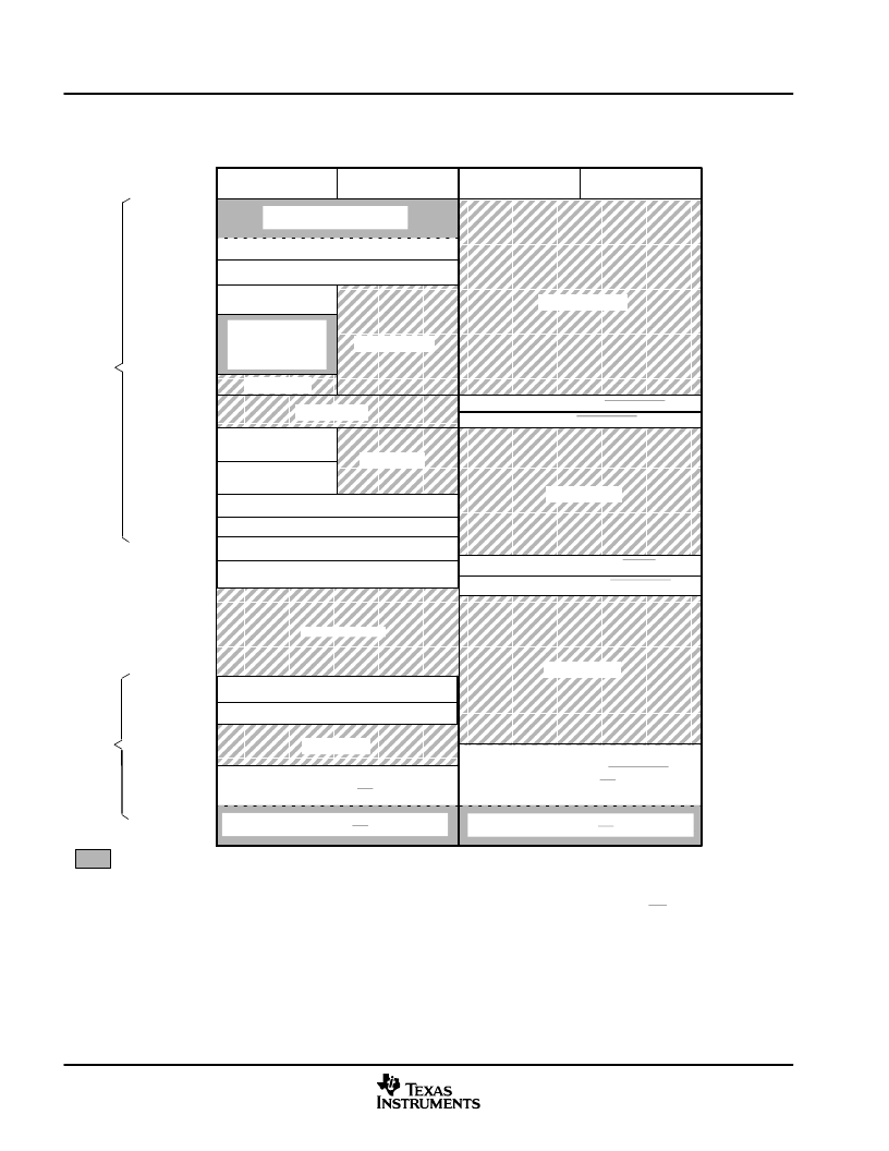
Functional Overview
28
June 2004
SPRS257
3.1
Memory Map
íííííííííííí
íííííííííííí
íííííííííííí
íííííííííííí
íííííííííííí
XINTF Zone 0 (8K
×
16, XZCS0AND1)
XINTF Zone 1 (8K
×
16, XZCS0AND1) (Protected)
ííííííííííííííííííííííí
ííííííííííííííííííííííí
íííííííííííí
(Enabled if MP/MC = 0)
íííííííííííí
ííííííííííííííííííííííí
(4K
×
16, Protected)
Block
Start Address
L
(
0x00 0000
M0 Vector
RAM (32
×
32)
(Enabled if VMAP = 0)
Data Space
Prog Space
M0 SARAM (1K
×
16)
M1 SARAM (1K
×
16)
ííííííííííííííííí
ííííííííííííííííí
ííííííííííííííííí
Reserved
Peripheral Frame 0
(2K
×
16)
PIE Vector - RAM
(256
×
16)
(Enabled if VMAP
= 1, ENPIE = 1)
0x00 0040
0x00 0400
0x00 0800
ííííííííííííííííííííííí
íííííííííííí
0x00 2000
Reserved
L0 SARAM (4K
×
16)
Peripheral Frame 1
ííííííííííííííííí
ííííííííííííííííí
Reserved
Peripheral Frame 2
(4K
×
16, Protected)
L1 SARAM (4K
×
16)
Reserved
BROM Vector - ROM (32
×
32)
(Enabled if VMAP = 1, MP/MC = 0, ENPIE = 0)
0x00 0D00
0x00 0E00
0x00 6000
0x00 7000
0x00 8000
0x00 9000
0x00 A000
0x00 A800
0x3F 8000
0x3F A000
0x3F F000
0x3F FFC0
H
(
P
Reserved
íííííííííííí
íííííííííííí
íííííííííííí
XINTF Zone 2 (0.5M
×
16, XZCS2)
XINTF Zone 7 (16K
×
16, XZCS6AND7)
(Enabled if MP/MC = 1)
XINTF Vector - RAM (32
×
32)
(Enabled if VMAP = 1, MP/MC = 1, ENPIE = 0)
On-Chip Memory
External Memory XINTF
Only one of these vector maps—M0 vector, PIE vector, BROM vector, XINTF vector—should be enabled at a time.
NOTES: A. Memory blocks are not to scale.
B. Reserved locations are reserved for future expansion. Application should not access these areas.
C. Boot ROM and Zone 7 memory maps are active either in on-chip or XINTF zone depending on MP/MC, not in both.
D. Peripheral Frame 0, Peripheral Frame 1, and Peripheral Frame 2 memory maps are restricted to data memory only.
User program cannot access these memory maps in program space.
E. “Protected” means the order of Write followed by Read operations is preserved rather than the pipeline order.
F. Certain memory ranges are EALLOW protected against spurious writes after configuration.
G. Zones 0 and 1 and Zones 6 and 7 share the same chip select; hence, these memory blocks have mirrored locations.
H. The passwords are set to all ones.
LEGEND:
0x08 0000
0x00 4000
0x10 0000
0x18 0000
0x3F C000
0x00 2000
ííííííííííííííííííííííí
ííííííííííííííííííííííí
ííííííííííííííííííííííí
ííííííííííííííííííííííí
ííííííííííííííííííííííí
Reserved
L2 SARAM (1K
×
16)
L3 SARAM (1K
×
16)
0x00 A400
0x3F7FF8
Figure 3
2. R2812 Memory Map (See Notes A through H)
A
相关PDF资料 |
PDF描述 |
|---|---|
| TMR320C2811GHHS | TMS320R2811, TMS320R2812 Digital Signal Processors |
| TMR320C2811PBKA | TMS320R2811, TMS320R2812 Digital Signal Processors |
| TMR320C2811PBKQ | TMS320R2811, TMS320R2812 Digital Signal Processors |
| TMR320C2811PBKS | TMS320R2811, TMS320R2812 Digital Signal Processors |
| TMR320C2811PGFA | TMS320R2811, TMS320R2812 Digital Signal Processors |
相关代理商/技术参数 |
参数描述 |
|---|---|
| TMR320C2811GHHS | 制造商:TI 制造商全称:Texas Instruments 功能描述:TMS320R2811, TMS320R2812 Digital Signal Processors |
| TMR320C2811PBKA | 制造商:TI 制造商全称:Texas Instruments 功能描述:TMS320R2811, TMS320R2812 Digital Signal Processors |
| TMR320C2811PBKQ | 制造商:TI 制造商全称:Texas Instruments 功能描述:TMS320R2811, TMS320R2812 Digital Signal Processors |
| TMR320C2811PBKS | 制造商:TI 制造商全称:Texas Instruments 功能描述:TMS320R2811, TMS320R2812 Digital Signal Processors |
| TMR320C2811PGFA | 制造商:TI 制造商全称:Texas Instruments 功能描述:TMS320R2811, TMS320R2812 Digital Signal Processors |
发布紧急采购,3分钟左右您将得到回复。