- 您现在的位置:买卖IC网 > PDF目录382635 > TMS29F800B-100BDCDL (Texas Instruments, Inc.) 1048576 BY 8-BIT/ 524288 BY 16-BIT FLASH MEMORIES PDF资料下载
参数资料
| 型号: | TMS29F800B-100BDCDL |
| 厂商: | Texas Instruments, Inc. |
| 英文描述: | 1048576 BY 8-BIT/ 524288 BY 16-BIT FLASH MEMORIES |
| 中文描述: | 1048576 8位/ 524288由16位闪存 |
| 文件页数: | 11/51页 |
| 文件大小: | 685K |
| 代理商: | TMS29F800B-100BDCDL |
第1页第2页第3页第4页第5页第6页第7页第8页第9页第10页当前第11页第12页第13页第14页第15页第16页第17页第18页第19页第20页第21页第22页第23页第24页第25页第26页第27页第28页第29页第30页第31页第32页第33页第34页第35页第36页第37页第38页第39页第40页第41页第42页第43页第44页第45页第46页第47页第48页第49页第50页第51页
TMS29F800T, TMS29F800B
1048576 BY 8-BIT/524288 BY 16-BIT
FLASH MEMORIES
SMJS835B – MAY 1997 – REVISED OCTOBER 1997
11
POST OFFICE BOX 1443
HOUSTON, TEXAS 77251–1443
read mode
A logic-low signal applied to the CE and OE pins allows the output of the TMS29F800T/B to be read. When two
or more ’29F800T/B devices are connected in parallel, the output of any one device can be read without
interference. The CE pin is for power control and must be used for device selection. The OE pin is for output
control and is used to gate the data output onto the bus from the selected device.
The address-access time (t
AVQV
) is the delay from stable address to valid output data. The chip-enable (CE)
access time (t
ELQV
) is the delay from CE low and stable addresses to valid output data. The output-enable
access time (t
GLQV
) is the delay from OE low to valid output data when CE equals logic low and addresses are
stable for at least the duration of t
AVQV
–t
GLQV
.
standby mode
I
CC
supply current is reduced by applying a logic-high level on CE and RESET to enter the standby mode. In
the standby mode, the outputs are placed in the high-impedance state. Applying a CMOS logic-high level on
CE and RESET reduces the current to 100
μ
A. Applying a TTL logic-high level on CE and RESET reduces the
current to 1 mA. If the ’29F800T/B is deselected during erasure or programming, the device continues to draw
active current until the operation is complete.
output disable
When OE equals V
IH
or CE equals V
IH
, output from the device is disabled and the output pins (DQ0–DQ15) are
placed in the high-impedance state.
automatic-sleep mode
The ’29F800 has a built-in feature called automatic-sleep mode to minimize device energy consumption which
is independent of CE, WE, and OE, and is enabled when addresses remain stable for 300 ns. Typical
sleep-mode current is 100
μ
A. Sleep mode does not affect output data, which remains latched and available
to the system.
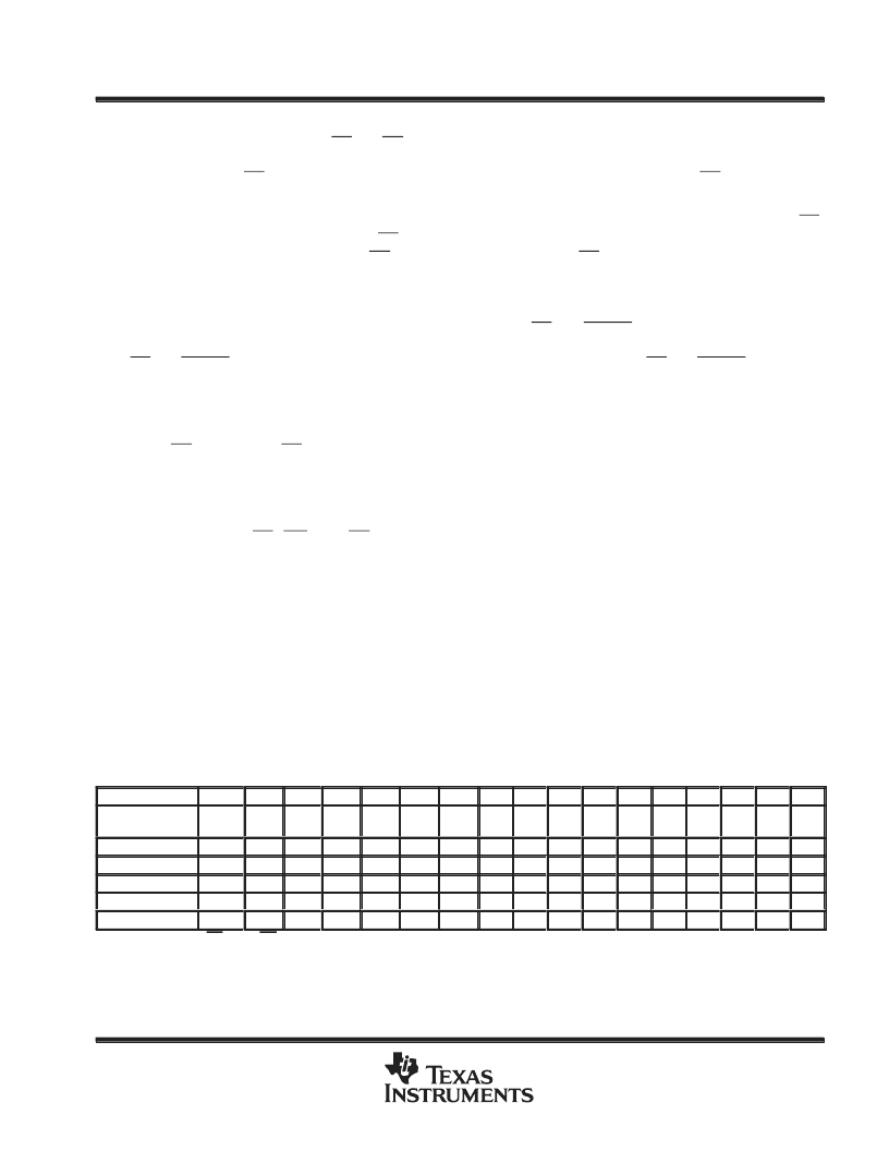
algorithm selection
The algorithm-selection mode provides access to a binary code that matches the device with its proper
programming and erase command operations. This mode is activated when V
ID
(11.5 V to 12.5 V) is placed on
address pin A9. Address pins A1 and A6 must be logic low. Two bytes of code are accessed by toggling address
pin A0 from V
IL
to V
IH
. Address pins other than A0, A1, and A6 can be at logic low or at logic high.
The algorithm-selection mode can also be read by using the command register, which is useful when V
ID
is not
available to be placed on address pin A9. Table 5 shows the binary algorithm-selection codes.
Table 5. Algorithm-Selection Codes (5-V Single Power Supply)
ááááááááááááááááááááááááááááá
ááááááááááááááááááááááááááááá
ááááááááááá
ááááááááááá
ááááááááá
A1 = VIL, A6 = VIL, CE = VIL, OE = VIL
CODE
DQ15
ááááááááá
A–1
A–1
Hi-Z
0
DQ14
ááááááááááááááááááááá
DQ13
DQ12
DQ11
áááááááááá
Hi-Z
DQ10
áááááá
DQ9
DQ8
ááááááááááá
Hi-Z
DQ7
áááááá
DQ6
DQ5
DQ4
DQ3
áááá
áááá
DQ2
DQ1
áá
áá
DQ0
Manufacturer-
58H
Hi-Z
0
0
0
1
1
1
0
2258H
ááááááá
1
áááááá
Hi-Z
Hi-Z
ááááááááááá
TMS29F800B–Byte
0
Hi-Z
Hi-Z
Hi-Z
1
0
1
0
1
0
0
0
0
ááááááááááááááááááááááááááááá
TMS29F800B
TMS29F800T
22D6H
0
1
0
0
0
1
0
0
1
1
1
0
0
1
0
1
0
1
0
0
ááááááááááááááááááááááááááááá
0
0
P
相关PDF资料 |
PDF描述 |
|---|---|
| TMS29F800B-100BDCDQ | PT 8C 8#20 PIN RECP |
| TMS29F800B-100CDBJE | RECEPT |
| TMS29F800B-100CDBJL | 1048576 BY 8-BIT/ 524288 BY 16-BIT FLASH MEMORIES |
| TMS29F800B-100CDBJQ | 1048576 BY 8-BIT/ 524288 BY 16-BIT FLASH MEMORIES |
| TMS29F800B-100CDCDE | 1048576 BY 8-BIT/ 524288 BY 16-BIT FLASH MEMORIES |
相关代理商/技术参数 |
参数描述 |
|---|---|
| TMS29F81606FML | 制造商:TI 功能描述:* |
| TMS-3/16-1.50-2 | 制造商:TE Connectivity 功能描述:5021710001 |
| TMS-3/16-1.50-3 | 制造商:TE Connectivity 功能描述:5023130001 |
| TMS-3/16-1.50-4 | 功能描述:电线鉴定 TMS-3/16-1.50-4 RoHS:否 制造商:TE Connectivity / Q-Cees 产品:Labels and Signs 类型: 材料:Vinyl 颜色:Blue 宽度:0.625 in 长度:1 in |
| TMS-3/16-1.50-4-CS7290 | 制造商:TE Connectivity 功能描述:502094N002 |
发布紧急采购,3分钟左右您将得到回复。