- 您现在的位置:买卖IC网 > PDF目录382626 > TMX320C2811PBKQ (Texas Instruments, Inc.) TMS320R2811, TMS320R2812 Digital Signal Processors PDF资料下载
参数资料
| 型号: | TMX320C2811PBKQ |
| 厂商: | Texas Instruments, Inc. |
| 元件分类: | 数字信号处理 |
| 英文描述: | TMS320R2811, TMS320R2812 Digital Signal Processors |
| 中文描述: | TMS320R2811,TMS320R2812数字信号处理器 |
| 文件页数: | 89/147页 |
| 文件大小: | 2021K |
| 代理商: | TMX320C2811PBKQ |
第1页第2页第3页第4页第5页第6页第7页第8页第9页第10页第11页第12页第13页第14页第15页第16页第17页第18页第19页第20页第21页第22页第23页第24页第25页第26页第27页第28页第29页第30页第31页第32页第33页第34页第35页第36页第37页第38页第39页第40页第41页第42页第43页第44页第45页第46页第47页第48页第49页第50页第51页第52页第53页第54页第55页第56页第57页第58页第59页第60页第61页第62页第63页第64页第65页第66页第67页第68页第69页第70页第71页第72页第73页第74页第75页第76页第77页第78页第79页第80页第81页第82页第83页第84页第85页第86页第87页第88页当前第89页第90页第91页第92页第93页第94页第95页第96页第97页第98页第99页第100页第101页第102页第103页第104页第105页第106页第107页第108页第109页第110页第111页第112页第113页第114页第115页第116页第117页第118页第119页第120页第121页第122页第123页第124页第125页第126页第127页第128页第129页第130页第131页第132页第133页第134页第135页第136页第137页第138页第139页第140页第141页第142页第143页第144页第145页第146页第147页
Electrical Specifications
89
June 2004
SPRS257
6.9
Timing Parameter Symbology
Timing parameter symbols used are created in accordance with JEDEC Standard 100. To shorten the
symbols, some of the pin names and other related terminology have been abbreviated as follows:
Lowercase subscripts and their meanings:
a
access time
c
cycle time (period)
d
delay time
f
fall time
h
hold time
r
rise time
su
setup time
t
transition time
v
valid time
w
pulse duration (width)
Letters and symbols and their meanings:
H
High
L
Low
V
Valid
X
Unknown, changing, or don’t care level
Z
High impedance
6.10
General Notes on Timing Parameters
All output signals from the 28x devices (including XCLKOUT) are derived from an internal clock such that all
output transitions for a given half-cycle occur with a minimum of skewing relative to each other.
The signal combinations shown in the following timing diagrams may not necessarily represent actual cycles.
For actual cycle examples, see the appropriate cycle description section of this document.
6.11
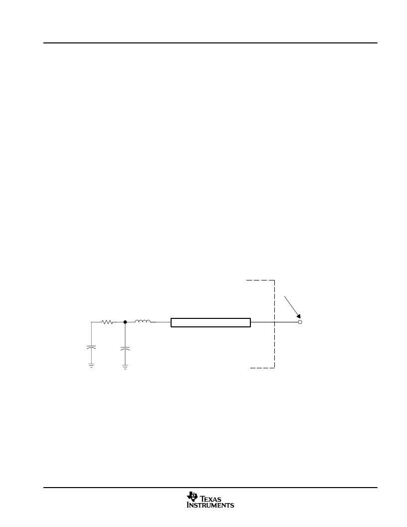
Test Load Circuit
This test load circuit is used to measure all switching characteristics provided in this document.
Transmission Line
4.0 pF
1.85 pF
Z0 = 50
(see note)
Tester Pin Electronics
Data Sheet Timing Reference Point
Output
Under
Test
NOTE: The data sheet provides timing at the device pin. For output timing analysis, the tester pin electronics and its transmission line effects
must be taken into account. A transmission line with a delay of 2 ns or longer can be used to produce the desired transmission line effect.
The transmission line is intended as a load only. It is not necessary to add or subtract the transmission line delay (2 ns or longer) from
the data sheet timing.
Input requirements in this data sheet are tested with an input slew rate of < 4 Volts per nanosecond (4 V/ns) at the device pin.
42
3.5 nH
Device Pin
(see note)
Figure 6
4. 3.3-V Test Load Circuit
A
相关PDF资料 |
PDF描述 |
|---|---|
| TMX320C2811PBKS | TMS320R2811, TMS320R2812 Digital Signal Processors |
| TMX320C2811PGFA | TMS320R2811, TMS320R2812 Digital Signal Processors |
| TMX320C2811PGFQ | TMS320R2811, TMS320R2812 Digital Signal Processors |
| TMX320C2811PGFS | TMS320R2811, TMS320R2812 Digital Signal Processors |
| TMX320C2811ZHHA | TMS320R2811, TMS320R2812 Digital Signal Processors |
相关代理商/技术参数 |
参数描述 |
|---|---|
| TMX320C2811PBKS | 制造商:TI 制造商全称:Texas Instruments 功能描述:TMS320R2811, TMS320R2812 Digital Signal Processors |
| TMX320C2811PGFA | 制造商:TI 制造商全称:Texas Instruments 功能描述:TMS320R2811, TMS320R2812 Digital Signal Processors |
| TMX320C2811PGFQ | 制造商:TI 制造商全称:Texas Instruments 功能描述:TMS320R2811, TMS320R2812 Digital Signal Processors |
| TMX320C2811PGFS | 制造商:TI 制造商全称:Texas Instruments 功能描述:TMS320R2811, TMS320R2812 Digital Signal Processors |
| TMX320C2811ZHHA | 制造商:TI 制造商全称:Texas Instruments 功能描述:TMS320R2811, TMS320R2812 Digital Signal Processors |
发布紧急采购,3分钟左右您将得到回复。