- 您现在的位置:买卖IC网 > PDF目录19748 > TNY279GN (Power Integrations)IC OFFLINE SWIT OVP OTP HV 8SMD PDF资料下载
参数资料
| 型号: | TNY279GN |
| 厂商: | Power Integrations |
| 文件页数: | 9/24页 |
| 文件大小: | 0K |
| 描述: | IC OFFLINE SWIT OVP OTP HV 8SMD |
| 标准包装: | 50 |
| 系列: | TinySwitch®-III |
| 输出隔离: | 隔离 |
| 频率范围: | 124kHz ~ 140kHz |
| 输出电压: | 700V |
| 功率(瓦特): | 32W |
| 工作温度: | -40°C ~ 150°C |
| 封装/外壳: | 8-SMD(7 个接脚),鸥形翼 |
| 供应商设备封装: | SMD-8C |
| 包装: | 管件 |
| 配用: | 596-1194-ND - KIT DESIGN REF TINYSWITCH-III |
�� �
�
�TNY274-280�
�Undervoltage� lockout� is� con?gured� by� R5� connected� between�
�the� DC� bus� and� EN/UV� pin� of� U1.� When� present,� switching� is�
�inhibited� until� the� current� in� the� EN/UV� pin� exceeds� 25� μ� A.� This�
�allows� the� startup� voltage� to� be� programmed� within� the� normal�
�operating� input� voltage� range,� preventing� glitching� of� the� output�
�under� abnormal� low� voltage� conditions� and� also� on� removal� of�
�the� AC� input.�
�8.� Increased� current� limit� is� selected� for� peak� and� open� frame�
�power� columns� and� standard� current� limit� for� adapter�
�columns.�
�9.� The� part� is� board� mounted� with� SOURCE� pins� soldered� to� a�
�suf?cient� area� of� copper� and/or� a� heatsink� is� used� to� keep�
�the� SOURCE� pin� temperature� at� or� below� 110� °C.�
�10.� Ambient� temperature� of� 50� °C� for� open� frame� designs� and�
�40� °C� for� sealed� adapters.�
�In� addition� to� the� simple� input� pi� ?lter� (C1,� L1,� C2)� for� differential�
�mode� EMI,� this� design� makes� use� of� E-Shield?� shielding�
�techniques� in� the� transformer� to� reduce� common� mode� EMI�
�displacement� currents,� and� R2� and� C4� as� a� damping� network�
�to� reduce� high� frequency� transformer� ringing.� These�
�techniques,� combined� with� the� frequency� jitter� of� TNY278,� give�
�excellent� conducted� and� radiated� EMI� performance� with� this�
�design� achieving� >12� dB� μ� V� of� margin� to� EN55022� Class� B�
�conducted� EMI� limits.�
�For� design� ?exibility� the� value� of� C7� can� be� selected� to� pick� one�
�of� the� 3� current� limits� options� in� U1.� This� allows� the� designer� to�
�select� the� current� limit� appropriate� for� the� application.�
�*Below� a� value� of� 1,� K� P� is� the� ratio� of� ripple� to� peak� primary�
�current.� To� prevent� reduced� power� capability� due� to� premature�
�termination� of� switching� cycles� a� transient� K� P� limit� of� ≥0.25� is�
�recommended.� This� prevents� the� initial� current� limit� (I� INIT� )� from�
�being� exceeded� at� MOSFET� turn� on.�
�For� reference,� Table� 2� provides� the� minimum� practical� power�
�delivered� from� each� family� member� at� the� three� selectable�
�current� limit� values.� This� assumes� open� frame� operation� (not�
�thermally� limited)� and� otherwise� the� same� conditions� as� listed�
�above.� These� numbers� are� useful� to� identify� the� correct� current�
�limit� to� select� for� a� given� device� and� output� power� requirement.�
�?�
�?�
�?�
�Standard� current� limit� (I� LIMIT� )� is� selected� with� a� 0.1� μ� F� BP/M� pin�
�capacitor� and� is� the� normal� choice� for� typical� enclosed�
�adapter� applications.�
�When� a� 1� μ� F� BP/M� pin� capacitor� is� used,� the� current� limit� is�
�reduced� (I� LIMITred� or� I� LIMIT� -1)� offering� reduced� RMS� device�
�currents� and� therefore� improved� ef?ciency,� but� at� the� expense�
�of� maximum� power� capability.� This� is� ideal� for� thermally�
�challenging� designs� where� dissipation� must� be� minimized.�
�When� a� 10� μ� F� BP/M� pin� capacitor� is� used,� the� current� limit� is�
�increased� (I� LIMITinc� or� I� LIMIT� +1),� extending� the� power� capability� for�
�applications� requiring� higher� peak� power� or� continuous� power�
�Overvoltage� Protection�
�The� output� overvoltage� protection� provided� by� TinySwitch-III�
�uses� an� internal� latch� that� is� triggered� by� a� threshold� current� of�
�approximately� 5.5� mA� into� the� BP/M� pin.� In� addition� to� an�
�internal� ?lter,� the� BP/M� pin� capacitor� forms� an� external� ?lter�
�providing� noise� immunity� from� inadvertent� triggering.� For� the�
�bypass� capacitor� to� be� effective� as� a� high� frequency� ?lter,� the�
�capacitor� should� be� located� as� close� as� possible� to� the�
�SOURCE� and� BP/M� pins� of� the� device.�
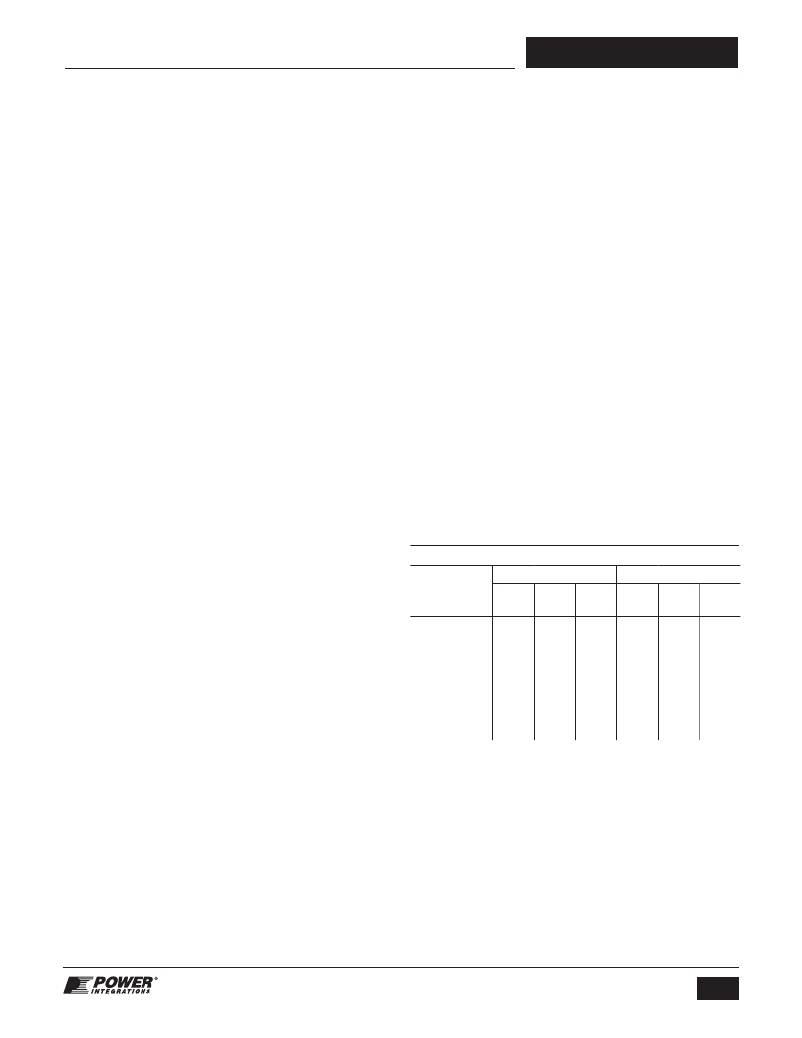
�Peak� Output� Power� Table�
�where� the� thermal� conditions� allow.�
�230� VAC� ±� 15%�
�85-265� VAC�
�Further� ?exibility� comes� from� the� current� limits� between�
�Product�
�I� LIMIT� -1�
�I� LIMIT�
�I� LIMIT� +1�
�I� LIMIT� -1�
�I� LIMIT�
�I� LIMIT� +1�
�adjacent� TinySwitch-III� family� members� being� compatible.� The�
�reduced� current� limit� of� a� given� device� is� equal� to� the� standard�
�current� limit� of� the� next� smaller� device� and� the� increased�
�TNY274P/G�
�TNY275P/G�
�8W�
�10.8� W�
�10.9� W�
�12� W�
�9.1� W�
�15.1� W�
�7.1� W�
�8.4� W�
�8.5� W�
�9.3� W�
�7.1� W�
�11.8� W�
�current� limit� is� equal� to� the� standard� current� limit� of� the� next�
�TNY276P/G�
�11.8� W� 15.3� W� 19.4� W�
�9.2� W�
�11.9� W� 15.1� W�
�larger� device.�
�TNY277P/G�
�15.1� W� 19.6� W� 23.7� W� 11.8� W� 15.3� W� 18.5� W�
�Key� Application� Considerations�
�TNY278P/G�
�19.4� W�
�24� W�
�28� W�
�15.1� W� 18.6� W� 21.8� W�
�TNY279P/G�
�23.7� W� 28.4� W� 32.2� W� 18.5� W�
�22� W�
�25.2� W�
�TinySwitch-lll� Design� Considerations�
�TNY280P/G�
�28� W�
�32.7� W� 36.6� W� 21.8� W� 25.4� W� 28.5� W�
�Output� Power� Table�
�The� data� sheet� output� power� table� (Table� 1)� represents� the�
�Table� 2.�
�Minimum� Practical� Power� at� Three� Selectable� Current� Limit� Levels.�
�minimum� practical� continuous� output� power� level� that� can� be�
�obtained� under� the� following� assumed� conditions:�
�1.� The� minimum� DC� input� voltage� is� 100� V� or� higher� for� 85� VAC�
�input,� or� 220� V� or� higher� for� 230� VAC� input� or� 115� VAC� with�
�a� voltage� doubler.� The� value� of� the� input� capacitance� should�
�be� sized� to� meet� these� criteria� for� AC� input� designs.�
�2.� Ef?ciency� of� 75%.�
�3.� Minimum� data� sheet� value� of� I� 2� f.�
�4.� Transformer� primary� inductance� tolerance� of� ±10%.�
�5.� Re?ected� output� voltage� (V� OR� )� of� 135� V.�
�6.� Voltage� only� output� of� 12� V� with� a� fast� PN� recti?er� diode.�
�7.� Continuous� conduction� mode� operation� with� transient� K� P� *�
�value� of� 0.25.�
�www.powerint.com�
�For� best� performance� of� the� OVP� function,� it� is� recommended�
�that� a� relatively� high� bias� winding� voltage� is� used,� in� the� range�
�of� 15� V-30� V.� This� minimizes� the� error� voltage� on� the� bias�
�winding� due� to� leakage� inductance� and� also� ensures� adequate�
�voltage� during� no-load� operation� from� which� to� supply� the�
�BP/M� pin� for� reduced� no-load� consumption.�
�Selecting� the� Zener� diode� voltage� to� be� approximately� 6� V�
�above� the� bias� winding� voltage� (28� V� for� 22� V� bias� winding)�
�gives� good� OVP� performance� for� most� designs,� but� can� be�
�adjusted� to� compensate� for� variations� in� leakage� inductance.�
�Adding� additional� ?ltering� can� be� achieved� by� inserting� a� low�
�9�
�Rev.� I� 01/09�
�相关PDF资料 |
PDF描述 |
|---|---|
| MIC29202BU TR | IC REG LDO ADJ .4A TO-263-5 |
| HMC36DRTN | CONN EDGECARD 72POS DIP .100 SLD |
| TAJC685M025RNJ | CAP TANT 6.8UF 25V 20% 2312 |
| HMC36DRTH | CONN EDGECARD 72POS DIP .100 SLD |
| LCMXO2280E-4T144C | IC PLD 2280LUTS 113I/O 144-TQFP |
相关代理商/技术参数 |
参数描述 |
|---|---|
| TNY279GN0152-TL | 制造商:Power Integrations 功能描述: |
| TNY279GN-TL | 功能描述:交流/直流开关转换器 25W 85-265 VAC 32W/230 VAC RoHS:否 制造商:STMicroelectronics 输出电压:800 V 输入/电源电压(最大值):23.5 V 输入/电源电压(最小值):11.5 V 开关频率:115 kHz 电源电流:1.6 mA 工作温度范围:- 40 C to + 150 C 安装风格:SMD/SMT 封装 / 箱体:SSO-10 封装:Reel |
| TNY279GTL | 制造商:POWERINT 制造商全称:Power Integrations, Inc. 功能描述:Energy Efficient, Off-Line Switcher with Enhanced Flexibility and Extended Power Range |
| TNY279P | 制造商:POWERINT 制造商全称:Power Integrations, Inc. 功能描述:Energy Efficient, Off-Line Switcher with Enhanced Flexibility and Extended Power Range |
| TNY279PG | 功能描述:交流/直流开关转换器 25 W (85-265 VAC) 32 W (230 VAC) RoHS:否 制造商:STMicroelectronics 输出电压:800 V 输入/电源电压(最大值):23.5 V 输入/电源电压(最小值):11.5 V 开关频率:115 kHz 电源电流:1.6 mA 工作温度范围:- 40 C to + 150 C 安装风格:SMD/SMT 封装 / 箱体:SSO-10 封装:Reel |
发布紧急采购,3分钟左右您将得到回复。